|
|
|
|
|
|
|
|
|
|
|
|
|
|
|
|
|
|
|
|
|
|
|
| DS5001FP | ||||||||
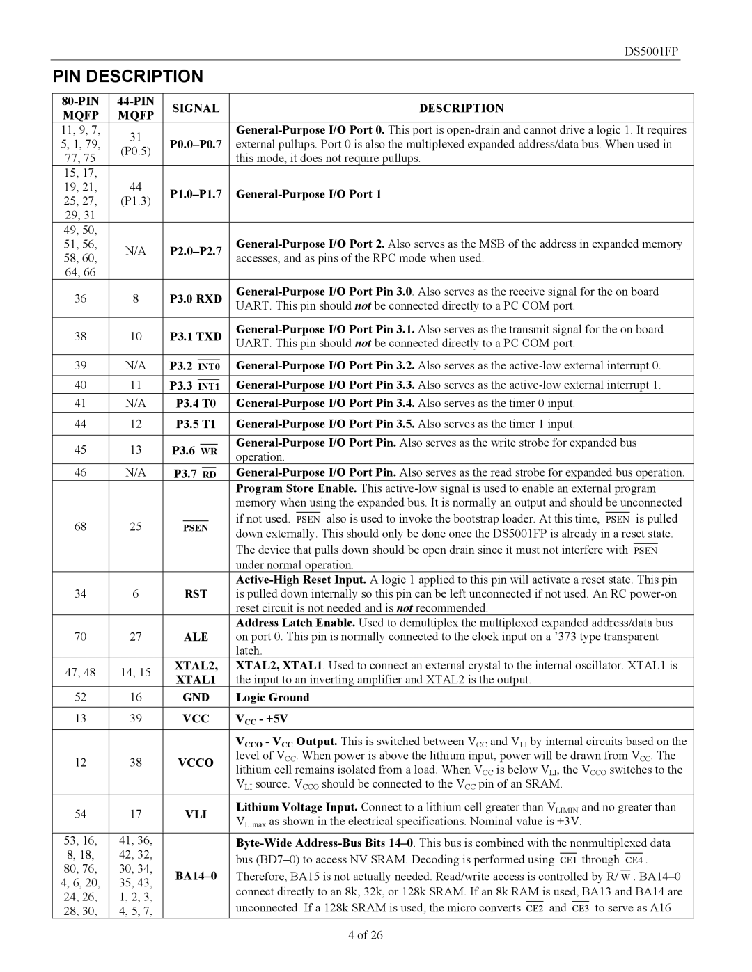
| PIN DESCRIPTION |
|
|
|
|
|
|
|
|
|
|
|
|
|
|
|
|
|
| |||||||||||||
|
|
|
|
|
|
|
|
|
|
|
|
|
|
|
|
|
|
|
|
|
|
|
|
|
|
|
|
|
|
|
| |
| SIGNAL |
|
| DESCRIPTION | ||||||||||||||||||||||||||||
| MQFP | MQFP |
|
| ||||||||||||||||||||||||||||
|
|
|
|
|
|
|
|
|
|
|
|
|
|
|
|
|
|
|
|
|
|
|
|
|
|
|
|
|
| |||
| 11, 9, 7, | 31 |
|
|
|
|
|
|
|
|
|
|
| |||||||||||||||||||
| 5, 1, 79, |
| external pullups. Port 0 is also the multiplexed expanded address/data bus. When used in | |||||||||||||||||||||||||||||
| (P0.5) | |||||||||||||||||||||||||||||||
| 77, 75 |
|
|
|
|
|
|
|
|
|
|
| this mode, it does not require pullups. | |||||||||||||||||||
|
|
|
|
|
|
|
|
|
|
|
|
| ||||||||||||||||||||
| 15, 17, | 44 |
|
|
|
|
|
|
|
|
|
|
|
|
|
|
|
|
|
|
|
|
|
|
|
|
|
|
|
|
| |
| 19, 21, | |||||||||||||||||||||||||||||||
| 25, 27, | (P1.3) | ||||||||||||||||||||||||||||||
|
|
|
|
|
|
|
|
|
|
|
|
|
|
|
|
|
|
|
|
|
|
|
|
|
|
|
|
|
| |||
| 29, 31 |
|
|
|
|
|
|
|
|
|
|
|
|
|
|
|
|
|
|
|
|
|
|
|
|
|
|
|
|
|
| |
| 49, 50, |
|
|
|
|
|
|
|
|
|
|
|
| |||||||||||||||||||
| 51, 56, | N/A | ||||||||||||||||||||||||||||||
| 58, 60, | accesses, and as pins of the RPC mode when used. | ||||||||||||||||||||||||||||||
|
|
|
|
|
|
|
|
|
|
|
|
| ||||||||||||||||||||
| 64, 66 |
|
|
|
|
|
|
|
|
|
|
|
|
|
|
|
|
|
|
|
|
|
|
|
|
|
|
|
|
|
| |
| 36 | 8 | P3.0 RXD | |||||||||||||||||||||||||||||
| UART. This pin should not be connected directly to a PC COM port. | |||||||||||||||||||||||||||||||
|
|
|
|
|
|
|
|
|
|
|
|
|
| |||||||||||||||||||
|
|
|
|
|
|
|
|
|
|
|
|
|
|
|
|
|
|
|
|
|
|
|
|
|
|
|
|
|
|
| ||
| 38 | 10 | P3.1 TXD | |||||||||||||||||||||||||||||
| UART. This pin should not be connected directly to a PC COM port. | |||||||||||||||||||||||||||||||
|
|
|
|
|
|
|
|
|
|
|
|
|
| |||||||||||||||||||
|
|
|
|
|
|
|
|
|
|
|
|
|
|
|
|
|
|
|
|
|
|
|
|
|
|
|
|
|
|
| ||
| 39 | N/A | P3.2 |
|
|
|
|
|
|
|
| |||||||||||||||||||||
INT0 | ||||||||||||||||||||||||||||||||
|
|
|
|
|
|
|
|
|
|
|
|
|
|
|
|
|
|
|
|
|
|
|
|
|
|
|
|
| ||||
| 40 | 11 | P3.3 |
|
|
|
|
|
|
|
|
| ||||||||||||||||||||
INT1 | ||||||||||||||||||||||||||||||||
| 41 | N/A | P3.4 T0 | |||||||||||||||||||||||||||||
| 44 | 12 | P3.5 T1 | |||||||||||||||||||||||||||||
|
|
|
|
|
|
|
|
|
|
|
|
|
|
|
|
|
|
|
|
|
|
|
|
|
|
|
|
|
|
| ||
| 45 | 13 |
|
|
|
|
|
|
|
|
|
|
| |||||||||||||||||||
| P3.6 WR | |||||||||||||||||||||||||||||||
| operation. | |||||||||||||||||||||||||||||||
|
|
|
|
|
|
|
|
|
|
|
|
|
| |||||||||||||||||||
| 46 | N/A | P3.7 |
|
|
| ||||||||||||||||||||||||||
RD | ||||||||||||||||||||||||||||||||
|
|
|
|
|
|
|
|
|
|
|
|
|
| Program Store Enable. This | ||||||||||||||||||
|
|
|
|
|
|
|
|
|
|
|
|
|
| memory when using the expanded bus. It is normally an output and should be unconnected | ||||||||||||||||||
|
|
|
|
|
|
|
|
|
|
|
|
|
| if not used. |
| also is used to invoke the bootstrap loader. At this time, |
|
|
|
|
| is pulled | ||||||||||
| 68 | 25 |
|
|
|
|
|
|
|
|
|
|
| PSEN | PSEN | |||||||||||||||||
| PSEN | |||||||||||||||||||||||||||||||
| down externally. This should only be done once the DS5001FP is already in a reset state. | |||||||||||||||||||||||||||||||
|
|
|
|
|
|
|
|
|
|
|
|
|
| |||||||||||||||||||
|
|
|
|
|
|
|
|
|
|
|
|
|
| The device that pulls down should be open drain since it must not interfere with |
|
|
| |||||||||||||||
|
|
|
|
|
|
|
|
|
|
|
|
|
| PSEN | ||||||||||||||||||
|
|
|
|
|
|
|
|
|
|
|
|
|
| under normal operation. | ||||||||||||||||||
|
|
|
|
|
|
|
|
|
|
|
|
|
| |||||||||||||||||||
| 34 | 6 |
| RST | is pulled down internally so this pin can be left unconnected if not used. An RC | |||||||||||||||||||||||||||
|
|
|
|
|
|
|
|
|
|
|
|
|
| reset circuit is not needed and is not recommended. | ||||||||||||||||||
|
|
|
|
|
|
|
|
|
|
|
|
|
| Address Latch Enable. Used to demultiplex the multiplexed expanded address/data bus | ||||||||||||||||||
| 70 | 27 |
| ALE | on port 0. This pin is normally connected to the clock input on a ’373 type transparent | |||||||||||||||||||||||||||
|
|
|
|
|
|
|
|
|
|
|
|
|
| latch. | ||||||||||||||||||
| 47, 48 | 14, 15 | XTAL2, | XTAL2, XTAL1. Used to connect an external crystal to the internal oscillator. XTAL1 is | ||||||||||||||||||||||||||||
| XTAL1 | the input to an inverting amplifier and XTAL2 is the output. | ||||||||||||||||||||||||||||||
|
|
| ||||||||||||||||||||||||||||||
| 52 | 16 | GND | Logic Ground | ||||||||||||||||||||||||||||
|
|
|
|
|
|
|
|
|
|
|
|
|
|
| ||||||||||||||||||
| 13 | 39 | VCC | VCC - +5V | ||||||||||||||||||||||||||||
|
|
|
|
|
|
|
|
|
|
|
|
|
| VCCO - VCC Output. This is switched between VCC and VLI by internal circuits based on the | ||||||||||||||||||
| 12 | 38 | VCCO | level of VCC. When power is above the lithium input, power will be drawn from VCC. The | ||||||||||||||||||||||||||||
| lithium cell remains isolated from a load. When VCC is below VLI, the VCCO switches to the | |||||||||||||||||||||||||||||||
|
|
|
|
|
|
|
|
|
|
|
|
|
| |||||||||||||||||||
|
|
|
|
|
|
|
|
|
|
|
|
|
| VLI source. VCCO should be connected to the VCC pin of an SRAM. | ||||||||||||||||||
| 54 | 17 |
| VLI | Lithium Voltage Input. Connect to a lithium cell greater than VLIMIN and no greater than | |||||||||||||||||||||||||||
|
| VLImax as shown in the electrical specifications. Nominal value is +3V. | ||||||||||||||||||||||||||||||
|
|
|
|
|
|
|
|
|
|
|
|
|
| |||||||||||||||||||
| 53, 16, | 41, 36, |
|
|
|
|
|
|
|
|
|
|
| |||||||||||||||||||
| 8, 18, | 42, 32, |
|
|
|
|
|
|
|
|
|
|
|
|
|
|
|
|
|
|
|
|
|
|
|
|
|
|
|
|
| |
|
|
|
|
|
|
|
|
|
|
| bus | |||||||||||||||||||||
| 80, 76, | 30, 34, |
|
|
|
|
|
|
|
|
|
|
| |||||||||||||||||||
|
|
|
|
|
|
|
|
|
|
|
|
|
|
|
|
|
|
| ||||||||||||||
Therefore, BA15 is not actually needed. Read/write access is controlled by R/ W . | ||||||||||||||||||||||||||||||||
| 4, 6, 20, | 35, 43, | ||||||||||||||||||||||||||||||
|
|
|
|
|
|
|
|
|
|
|
| connect directly to an 8k, 32k, or 128k SRAM. If an 8k RAM is used, BA13 and BA14 are | ||||||||||||||||||||
| 24, 26, | 1, 2, 3, |
|
|
|
|
|
|
|
|
|
|
| |||||||||||||||||||
|
|
|
|
|
|
|
|
|
|
|
| unconnected. If a 128k SRAM is used, the micro converts |
| and |
|
| to serve as A16 | |||||||||||||||
| 28, 30, | 4, 5, 7, |
|
|
|
|
|
|
|
|
|
|
| CE2 | CE3 | |||||||||||||||||
4 of 26