|
|
|
|
|
|
|
|
|
|
|
|
|
|
|
|
|
|
|
|
|
|
|
|
|
|
|
|
|
|
|
|
|
|
|
|
|
| DS5001FP | ||||
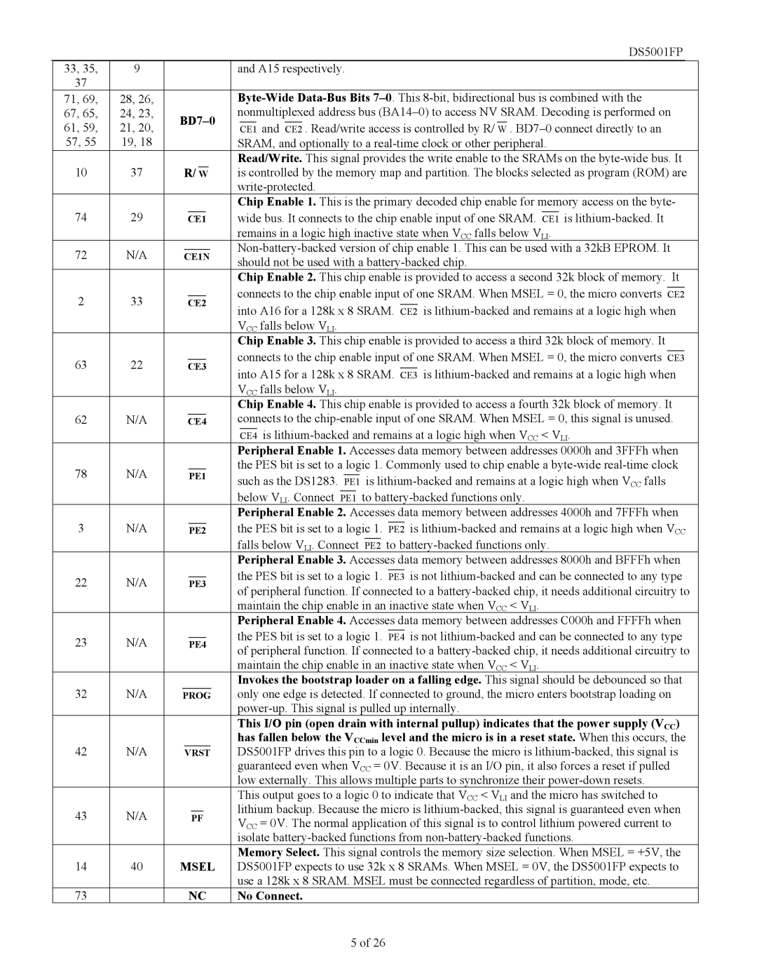
| 33, 35, | 9 |
|
|
|
|
|
|
|
|
|
|
|
|
|
|
| and A15 respectively. |
| |||||||||||||||||||||||
| 37 |
|
|
|
|
|
|
|
|
|
|
|
|
|
|
|
|
|
|
|
|
|
|
|
|
|
|
|
|
|
|
|
|
|
|
|
|
|
|
|
|
|
| 71, 69, | 28, 26, |
|
|
|
|
|
|
|
|
|
|
|
|
|
|
| |||||||||||||||||||||||||
| 67, 65, | 24, 23, |
| nonmultiplexed address bus | ||||||||||||||||||||||||||||||||||||||
| 61, 59, | 21, 20, |
|
|
|
|
|
|
|
|
|
|
|
|
|
|
|
|
|
|
|
|
|
|
|
|
| |||||||||||||||
| CE1 and CE2 . Read/write access is controlled by R/ W . | |||||||||||||||||||||||||||||||||||||||||
|
|
|
|
|
|
|
|
|
|
|
|
|
|
|
| |||||||||||||||||||||||||||
| 57, 55 | 19, 18 |
|
|
|
|
|
|
|
|
|
|
|
|
|
|
| SRAM, and optionally to a | ||||||||||||||||||||||||
|
|
|
|
|
|
|
|
|
|
|
|
|
|
|
|
|
| Read/Write. This signal provides the write enable to the SRAMs on the | ||||||||||||||||||||||||
| 10 | 37 |
| R/ |
|
|
|
|
|
|
|
|
| is controlled by the memory map and partition. The blocks selected as program (ROM) are | ||||||||||||||||||||||||||||
W | ||||||||||||||||||||||||||||||||||||||||||
|
|
|
|
|
|
|
|
|
|
|
|
|
|
|
|
|
| |||||||||||||||||||||||||
| 74 | 29 |
|
|
|
|
|
|
|
|
|
|
|
|
|
|
| Chip Enable 1. This is the primary decoded chip enable for memory access on the byte- | ||||||||||||||||||||||||
|
|
|
|
|
|
|
|
|
|
|
|
| wide bus. It connects to the chip enable input of one SRAM. |
| is | |||||||||||||||||||||||||||
|
|
| CE1 |
|
|
|
|
|
|
| CE1 | |||||||||||||||||||||||||||||||
|
|
|
|
|
|
|
|
|
|
|
|
|
|
|
|
|
| remains in a logic high inactive state when VCC falls below VLI. | ||||||||||||||||||||||||
| 72 | N/A |
|
|
|
|
|
|
|
|
|
|
|
|
|
|
| |||||||||||||||||||||||||
|
| CE1N | ||||||||||||||||||||||||||||||||||||||||
|
| should not be used with a | ||||||||||||||||||||||||||||||||||||||||
|
|
|
|
|
|
|
|
|
|
|
|
|
|
|
|
|
| |||||||||||||||||||||||||
|
|
|
|
|
|
|
|
|
|
|
|
|
|
|
|
|
| Chip Enable 2. This chip enable is provided to access a second 32k block of memory. It | ||||||||||||||||||||||||
|
|
|
|
|
|
|
|
|
|
|
|
|
|
|
|
|
| connects to the chip enable input of one SRAM. When MSEL = 0, the micro converts |
|
|
| |||||||||||||||||||||
| 2 | 33 |
|
|
|
|
|
|
|
|
|
|
|
|
|
|
| CE2 | ||||||||||||||||||||||||
|
|
| CE2 | |||||||||||||||||||||||||||||||||||||||
|
|
|
|
|
|
|
|
|
|
|
|
|
|
|
|
|
|
|
|
|
|
|
|
|
|
|
| |||||||||||||||
|
| into A16 for a 128k x 8 SRAM. CE2 is | ||||||||||||||||||||||||||||||||||||||||
|
|
|
|
|
|
|
|
|
|
|
|
|
|
|
|
|
| |||||||||||||||||||||||||
|
|
|
|
|
|
|
|
|
|
|
|
|
|
|
|
|
| VCC falls below VLI. | ||||||||||||||||||||||||
|
|
|
|
|
|
|
|
|
|
|
|
|
|
|
|
|
| Chip Enable 3. This chip enable is provided to access a third 32k block of memory. It | ||||||||||||||||||||||||
|
|
|
|
|
|
|
|
|
|
|
|
|
|
|
|
|
| connects to the chip enable input of one SRAM. When MSEL = 0, the micro converts |
|
| ||||||||||||||||||||||
| 63 | 22 |
|
|
|
|
|
|
|
|
|
|
|
|
|
|
| CE3 | ||||||||||||||||||||||||
|
|
| CE3 | |||||||||||||||||||||||||||||||||||||||
|
|
|
|
|
|
|
|
|
|
|
|
|
|
|
|
|
|
|
|
|
|
|
|
|
|
|
| |||||||||||||||
|
| into A15 for a 128k x 8 SRAM. CE3 is | ||||||||||||||||||||||||||||||||||||||||
|
|
|
|
|
|
|
|
|
|
|
|
|
|
|
|
|
| |||||||||||||||||||||||||
|
|
|
|
|
|
|
|
|
|
|
|
|
|
|
|
|
| VCC falls below VLI. | ||||||||||||||||||||||||
|
|
|
|
|
|
|
|
|
|
|
|
|
|
|
|
|
| Chip Enable 4. This chip enable is provided to access a fourth 32k block of memory. It | ||||||||||||||||||||||||
| 62 | N/A |
|
|
|
|
|
|
|
|
|
| connects to the | |||||||||||||||||||||||||||||
|
|
| CE4 |
|
|
|
| |||||||||||||||||||||||||||||||||||
|
|
|
|
|
|
|
|
|
|
|
|
|
|
|
|
|
|
| CE4 | is | ||||||||||||||||||||||
|
|
|
|
|
|
|
|
|
|
|
|
|
|
|
|
|
| Peripheral Enable 1. Accesses data memory between addresses 0000h and 3FFFh when | ||||||||||||||||||||||||
| 78 | N/A |
|
|
|
|
|
|
|
|
|
|
|
|
|
|
| the PES bit is set to a logic 1. Commonly used to chip enable a | ||||||||||||||||||||||||
|
|
|
|
| PE1 |
|
|
|
|
|
|
|
|
|
|
|
|
|
|
|
|
|
|
|
|
|
|
|
|
|
|
|
|
| ||||||||
|
|
|
|
|
|
|
|
|
| such as the DS1283. PE1 is | ||||||||||||||||||||||||||||||||
|
|
|
|
|
|
|
|
|
|
|
|
|
|
|
|
|
| |||||||||||||||||||||||||
|
|
|
|
|
|
|
|
|
|
|
|
|
|
|
|
|
| below VLI. Connect |
| to | ||||||||||||||||||||||
|
|
|
|
|
|
|
|
|
|
|
|
|
|
|
|
|
| PE1 | ||||||||||||||||||||||||
|
|
|
|
|
|
|
|
|
|
|
|
|
|
|
|
|
| Peripheral Enable 2. Accesses data memory between addresses 4000h and 7FFFh when | ||||||||||||||||||||||||
| 3 | N/A |
|
|
|
|
|
|
|
| the PES bit is set to a logic 1. |
|
|
| is | |||||||||||||||||||||||||||
|
|
|
|
|
|
|
|
|
|
|
|
|
|
| PE2 | |||||||||||||||||||||||||||
|
|
|
| PE2 |
|
|
| |||||||||||||||||||||||||||||||||||
|
|
|
|
|
|
|
|
|
|
|
|
|
|
|
|
|
| falls below VLI. Connect |
| to | ||||||||||||||||||||||
|
|
|
|
|
|
|
|
|
|
|
|
|
|
|
|
|
| PE2 | ||||||||||||||||||||||||
|
|
|
|
|
|
|
|
|
|
|
|
|
|
|
|
|
| Peripheral Enable 3. Accesses data memory between addresses 8000h and BFFFh when | ||||||||||||||||||||||||
|
|
|
|
|
|
|
|
|
|
|
|
|
|
|
|
|
| the PES bit is set to a logic 1. |
| is not | ||||||||||||||||||||||
| 22 | N/A |
|
|
|
|
|
|
|
|
|
|
|
|
|
|
| PE3 | ||||||||||||||||||||||||
|
|
|
| PE3 | ||||||||||||||||||||||||||||||||||||||
|
|
|
| of peripheral function. If connected to a | ||||||||||||||||||||||||||||||||||||||
|
|
|
|
|
|
|
|
|
|
|
|
|
|
|
|
|
| |||||||||||||||||||||||||
|
|
|
|
|
|
|
|
|
|
|
|
|
|
|
|
|
| maintain the chip enable in an inactive state when VCC < VLI. | ||||||||||||||||||||||||
|
|
|
|
|
|
|
|
|
|
|
|
|
|
|
|
|
| Peripheral Enable 4. Accesses data memory between addresses C000h and FFFFh when | ||||||||||||||||||||||||
|
|
|
|
|
|
|
|
|
|
|
|
|
|
|
|
|
| the PES bit is set to a logic 1. |
| is not | ||||||||||||||||||||||
| 23 | N/A |
|
|
|
|
|
|
|
|
|
|
|
|
|
|
| PE4 | ||||||||||||||||||||||||
|
|
|
| PE4 | ||||||||||||||||||||||||||||||||||||||
|
|
|
| of peripheral function. If connected to a | ||||||||||||||||||||||||||||||||||||||
|
|
|
|
|
|
|
|
|
|
|
|
|
|
|
|
|
| |||||||||||||||||||||||||
|
|
|
|
|
|
|
|
|
|
|
|
|
|
|
|
|
| maintain the chip enable in an inactive state when VCC < VLI. | ||||||||||||||||||||||||
|
|
|
|
|
|
|
|
|
|
|
|
|
|
|
|
|
| Invokes the bootstrap loader on a falling edge. This signal should be debounced so that | ||||||||||||||||||||||||
| 32 | N/A |
| PROG |
| only one edge is detected. If connected to ground, the micro enters bootstrap loading on | ||||||||||||||||||||||||||||||||||||
|
|
|
|
|
|
|
|
|
|
|
|
|
|
|
|
|
| |||||||||||||||||||||||||
|
|
|
|
|
|
|
|
|
|
|
|
|
|
|
|
|
| This I/O pin (open drain with internal pullup) indicates that the power supply (VCC) | ||||||||||||||||||||||||
|
|
|
|
|
|
|
|
|
|
|
|
|
|
|
|
|
| has fallen below the VCCmin level and the micro is in a reset state. When this occurs, the | ||||||||||||||||||||||||
| 42 | N/A |
|
| VRST |
| DS5001FP drives this pin to a logic 0. Because the micro is | |||||||||||||||||||||||||||||||||||
|
|
|
|
|
|
|
|
|
|
|
|
|
|
|
|
|
| guaranteed even when VCC = 0V. Because it is an I/O pin, it also forces a reset if pulled | ||||||||||||||||||||||||
|
|
|
|
|
|
|
|
|
|
|
|
|
|
|
|
|
| low externally. This allows multiple parts to synchronize their | ||||||||||||||||||||||||
|
|
|
|
|
|
|
|
|
|
|
|
|
|
|
|
|
| This output goes to a logic 0 to indicate that VCC < VLI and the micro has switched to | ||||||||||||||||||||||||
| 43 | N/A |
|
|
|
|
|
|
|
|
|
|
|
|
|
|
| lithium backup. Because the micro is | ||||||||||||||||||||||||
|
|
|
|
| PF | |||||||||||||||||||||||||||||||||||||
|
|
|
|
| VCC = 0V. The normal application of this signal is to control lithium powered current to | |||||||||||||||||||||||||||||||||||||
|
|
|
|
|
|
|
|
|
|
|
|
|
|
|
|
|
| |||||||||||||||||||||||||
|
|
|
|
|
|
|
|
|
|
|
|
|
|
|
|
|
| isolate | ||||||||||||||||||||||||
|
|
|
|
|
|
|
|
|
|
|
|
|
|
|
|
|
| Memory Select. This signal controls the memory size selection. When MSEL = +5V, the | ||||||||||||||||||||||||
| 14 | 40 | MSEL | DS5001FP expects to use 32k x 8 SRAMs. When MSEL = 0V, the DS5001FP expects to | ||||||||||||||||||||||||||||||||||||||
|
|
|
|
|
|
|
|
|
|
|
|
|
|
|
|
|
| use a 128k x 8 SRAM. MSEL must be connected regardless of partition, mode, etc. | ||||||||||||||||||||||||
| 73 |
|
|
|
| NC | No Connect. | |||||||||||||||||||||||||||||||||||
5 of 26