AT INTERFACE DESCRIPTION
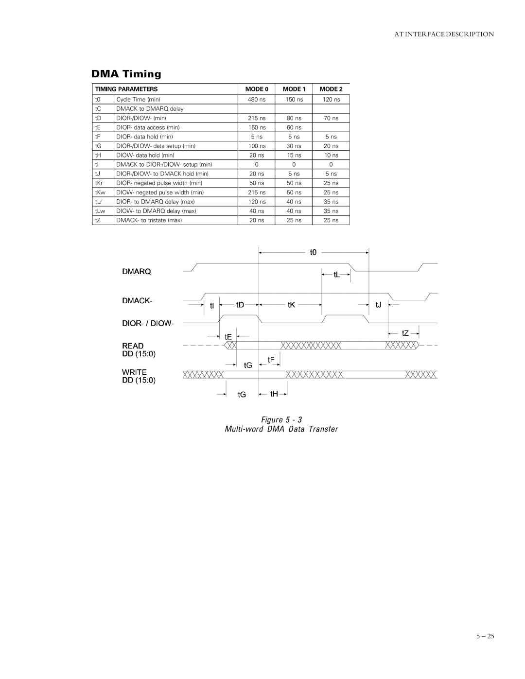
DMA Timing
TIMING PARAMETERS | MODE 0 | MODE 1 | MODE 2 | |
|
|
|
|
|
t0 | Cycle Time (min) | 480 ns | 150 ns | 120 ns |
tC | DMACK to DMARQ delay |
|
|
|
|
|
|
|
|
tD | 215 ns | 80 ns | 70 ns | |
tE | DIOR- data access (min) | 150 ns | 60 ns |
|
tF | DIOR- data hold (min) | 5 ns | 5 ns | 5 ns |
tG | 100 ns | 30 ns | 20 ns | |
|
|
|
|
|
tH | DIOW- data hold (min) | 20 ns | 15 ns | 10 ns |
tI | DMACK to | 0 | 0 | 0 |
|
|
|
|
|
tJ | 20 ns | 5 ns | 5 ns | |
tKr | DIOR- negated pulse width (min) | 50 ns | 50 ns | 25 ns |
tKw | DIOW- negated pulse width (min) | 215 ns | 50 ns | 25 ns |
tLr | DIOR- to DMARQ delay (max) | 120 ns | 40 ns | 35 ns |
tLw | DIOW- to DMARQ delay (max) | 40 ns | 40 ns | 35 ns |
|
|
|
|
|
tZ | DMACK- to tristate (max) | 20 ns | 25 ns | 25 ns |
Figure 5 - 3 |
5 – 25