Specifications |
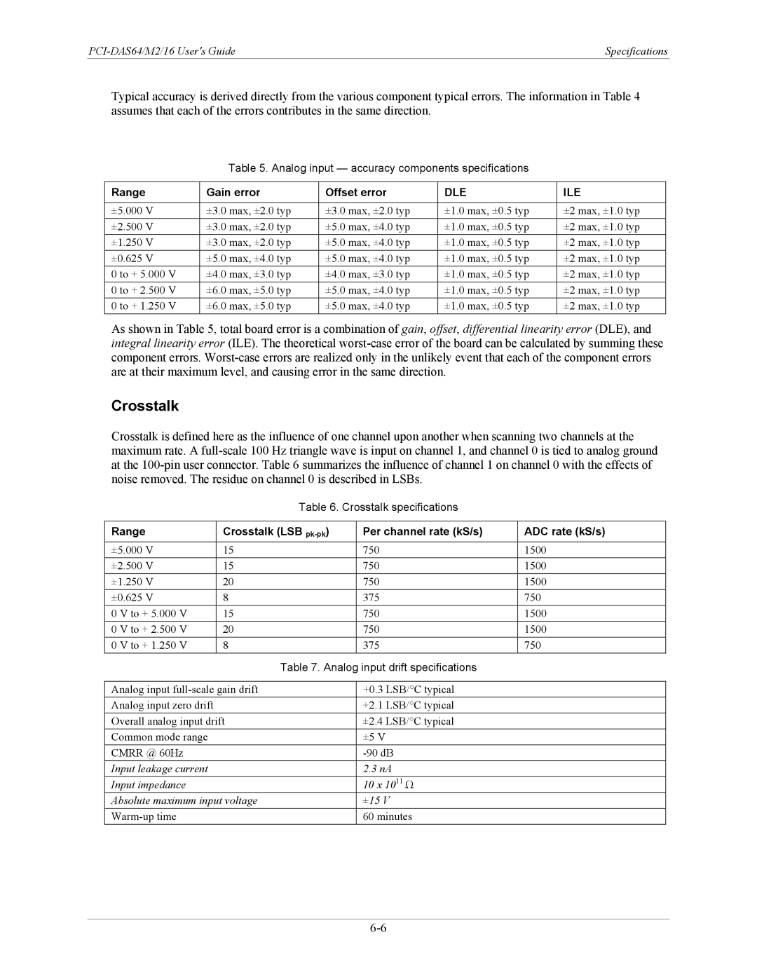
Typical accuracy is derived directly from the various component typical errors. The information in Table 4 assumes that each of the errors contributes in the same direction.
Table 5. Analog input — accuracy components specifications
Range | Gain error | Offset error | DLE | ILE |
|
|
|
|
|
±5.000 V | ±3.0 max, ±2.0 typ | ±3.0 max, ±2.0 typ | ±1.0 max, ±0.5 typ | ±2 max, ±1.0 typ |
±2.500 V | ±3.0 max, ±2.0 typ | ±5.0 max, ±4.0 typ | ±1.0 max, ±0.5 typ | ±2 max, ±1.0 typ |
±1.250 V | ±3.0 max, ±2.0 typ | ±5.0 max, ±4.0 typ | ±1.0 max, ±0.5 typ | ±2 max, ±1.0 typ |
±0.625 V | ±5.0 max, ±4.0 typ | ±5.0 max, ±4.0 typ | ±1.0 max, ±0.5 typ | ±2 max, ±1.0 typ |
0 to + 5.000 V | ±4.0 max, ±3.0 typ | ±4.0 max, ±3.0 typ | ±1.0 max, ±0.5 typ | ±2 max, ±1.0 typ |
0 to + 2.500 V | ±6.0 max, ±5.0 typ | ±5.0 max, ±4.0 typ | ±1.0 max, ±0.5 typ | ±2 max, ±1.0 typ |
0 to + 1.250 V | ±6.0 max, ±5.0 typ | ±5.0 max, ±4.0 typ | ±1.0 max, ±0.5 typ | ±2 max, ±1.0 typ |
As shown in Table 5, total board error is a combination of gain, offset, differential linearity error (DLE), and integral linearity error (ILE). The theoretical
Crosstalk
Crosstalk is defined here as the influence of one channel upon another when scanning two channels at the maximum rate. A
Table 6. Crosstalk specifications
Range | Crosstalk (LSB | Per channel rate (kS/s) | ADC rate (kS/s) |
|
|
|
|
±5.000 V | 15 | 750 | 1500 |
±2.500 V | 15 | 750 | 1500 |
±1.250 V | 20 | 750 | 1500 |
±0.625 V | 8 | 375 | 750 |
0 V to + 5.000 V | 15 | 750 | 1500 |
0 V to + 2.500 V | 20 | 750 | 1500 |
0 V to + 1.250 V | 8 | 375 | 750 |
| Table 7. Analog input drift specifications |
| |
|
|
| |
Analog input | +0.3 LSB/°C typical |
| |
Analog input zero drift |
| +2.1 LSB/°C typical |
|
Overall analog input drift | ±2.4 LSB/°C typical |
| |
Common mode range |
| ±5 V |
|
CMRR @ 60Hz |
|
| |
Input leakage current |
| 2.3 nA |
|
Input impedance |
| 10 x 1011 Ω |
|
Absolute maximum input voltage | ±15 V |
| |
| 60 minutes |
| |