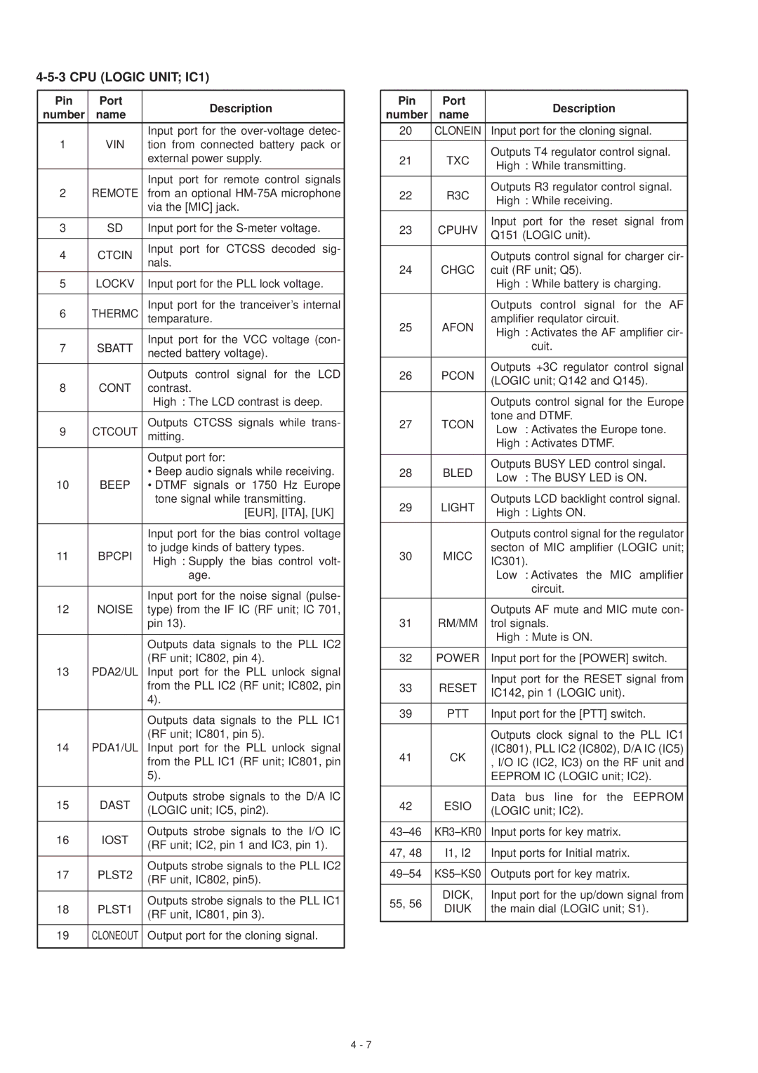
4-5-3 CPU (LOGIC UNIT; IC1)
Pin | Port | Description | |
number | name | ||
| |||
|
| Input port for the | |
1 | VIN | tion from connected battery pack or | |
|
| external power supply. | |
|
|
| |
|
| Input port for remote control signals | |
2 | REMOTE | from an optional | |
|
| via the [MIC] jack. | |
|
|
| |
3 | SD | Input port for the | |
|
|
| |
4 | CTCIN | Input port for CTCSS decoded sig- | |
nals. | |||
|
| ||
|
|
| |
5 | LOCKV | Input port for the PLL lock voltage. | |
|
|
| |
6 | THERMC | Input port for the tranceiver’s internal | |
temparature. | |||
|
|
| |
7 | SBATT | Input port for the VCC voltage (con- | |
nected battery voltage). | |||
|
| ||
|
|
| |
|
| Outputs control signal for the LCD | |
8 | CONT | contrast. | |
|
| High : The LCD contrast is deep. | |
|
|
| |
9 | CTCOUT | Outputs CTCSS signals while trans- | |
mitting. | |||
|
|
| |
|
| Output port for: | |
|
| • Beep audio signals while receiving. | |
10 | BEEP | • DTMF signals or 1750 Hz Europe | |
|
| tone signal while transmitting. | |
|
| [EUR], [ITA], [UK] | |
|
|
| |
|
| Input port for the bias control voltage | |
11 | BPCPI | to judge kinds of battery types. | |
High : Supply the bias control volt- | |||
|
| ||
|
| age. | |
|
|
| |
|
| Input port for the noise signal (pulse- | |
12 | NOISE | type) from the IF IC (RF unit; IC 701, | |
|
| pin 13). | |
|
|
| |
|
| Outputs data signals to the PLL IC2 | |
|
| (RF unit; IC802, pin 4). | |
13 | PDA2/UL | Input port for the PLL unlock signal | |
|
| from the PLL IC2 (RF unit; IC802, pin | |
|
| 4). | |
|
|
| |
|
| Outputs data signals to the PLL IC1 | |
|
| (RF unit; IC801, pin 5). | |
14 | PDA1/UL | Input port for the PLL unlock signal | |
|
| from the PLL IC1 (RF unit; IC801, pin | |
|
| 5). | |
|
|
| |
15 | DAST | Outputs strobe signals to the D/A IC | |
(LOGIC unit; IC5, pin2). | |||
|
| ||
|
|
| |
16 | IOST | Outputs strobe signals to the I/O IC | |
(RF unit; IC2, pin 1 and IC3, pin 1). | |||
|
| ||
|
|
| |
17 | PLST2 | Outputs strobe signals to the PLL IC2 | |
(RF unit, IC802, pin5). | |||
|
| ||
|
|
| |
18 | PLST1 | Outputs strobe signals to the PLL IC1 | |
(RF unit, IC801, pin 3). | |||
|
| ||
|
|
| |
19 | CLONEOUT | Output port for the cloning signal. | |
|
|
|
Pin | Port | Description | |
number | name | ||
| |||
20 | CLONEIN | Input port for the cloning signal. | |
|
|
| |
21 | TXC | Outputs T4 regulator control signal. | |
High : While transmitting. | |||
|
| ||
|
|
| |
22 | R3C | Outputs R3 regulator control signal. | |
High : While receiving. | |||
|
| ||
|
|
| |
23 | CPUHV | Input port for the reset signal from | |
Q151 (LOGIC unit). | |||
|
| ||
|
|
| |
|
| Outputs control signal for charger cir- | |
24 | CHGC | cuit (RF unit; Q5). | |
|
| High : While battery is charging. | |
|
|
| |
|
| Outputs control signal for the AF | |
25 | AFON | amplifier requlator circuit. | |
High : Activates the AF amplifier cir- | |||
|
| ||
|
| cuit. | |
|
|
| |
26 | PCON | Outputs +3C regulator control signal | |
(LOGIC unit; Q142 and Q145). | |||
|
| ||
|
|
| |
|
| Outputs control signal for the Europe | |
27 | TCON | tone and DTMF. | |
Low : Activates the Europe tone. | |||
|
| ||
|
| High : Activates DTMF. | |
|
|
| |
28 | BLED | Outputs BUSY LED control singal. | |
Low : The BUSY LED is ON. | |||
|
| ||
|
|
| |
29 | LIGHT | Outputs LCD backlight control signal. | |
High : Lights ON. | |||
|
| ||
|
|
| |
|
| Outputs control signal for the regulator | |
30 | MICC | secton of MIC amplifier (LOGIC unit; | |
IC301). | |||
|
| ||
|
| Low : Activates the MIC amplifier | |
|
| circuit. | |
|
|
| |
|
| Outputs AF mute and MIC mute con- | |
31 | RM/MM | trol signals. | |
|
| High : Mute is ON. | |
|
|
| |
32 | POWER | Input port for the [POWER] switch. | |
|
|
| |
33 | RESET | Input port for the RESET signal from | |
IC142, pin 1 (LOGIC unit). | |||
|
| ||
|
|
| |
39 | PTT | Input port for the [PTT] switch. | |
|
|
| |
|
| Outputs clock signal to the PLL IC1 | |
41 | CK | (IC801), PLL IC2 (IC802), D/A IC (IC5) | |
, I/O IC (IC2, IC3) on the RF unit and | |||
|
| ||
|
| EEPROM IC (LOGIC unit; IC2). | |
|
|
| |
42 | ESIO | Data bus line for the EEPROM | |
(LOGIC unit; IC2). | |||
|
| ||
|
|
| |
Input ports for key matrix. | |||
|
|
| |
47, 48 | I1, I2 | Input ports for Initial matrix. | |
|
|
| |
Outputs port for key matrix. | |||
|
|
| |
55, 56 | DICK, | Input port for the up/down signal from | |
DIUK | the main dial (LOGIC unit; S1). | ||
| |||
|
|
|
4 - 7