• RF signals WFM band | • 50, 144, 440 and 1200 MHz band |
The WFM band signals are applied to the RF amplifier (Q201) via the tunable
Varactor diodes (D106, D107, D202, D203, D306, D309, D310) are employed by the tunable bandpass filter to tune the center frequency of the bandpass filter. These diodes are controlled by the PLL lock voltage and obtain good image response rejection.
4-1-5 440 MHz BAND RF CIRCUIT (RF UNIT)
The signals from the antenna switching circuit (D402 and D403) are amplified at the RF amplifier (Q401). The ampli- fied signals pass through the bandpass filter (FI401), and are then applied to the 1st mixer circuit (IC601, pin 1) after being amplified at another RF amplifier (IC501).
4-1-6 1200 MHz BAND RF CIRCUIT (RF UNIT)
The signals from the antenna switching circuit (D51 and D52) are amplified at the RF amplifier (Q51). The amplified signals pass through the bandpass filter (FI51), and are then applied to the RF amplifier (IC51). The amplified signal is applied to the 1st mixer circuit (IC601, pin 1) via the band- pass filter (FI52).
4-1-7 1ST MIXER CIRCUIT (RF UNIT)
The 1st mixer circuit converts the received RF signals into a fixed frequency of the 1st IF signal with a 1st LO output fre- quency. By changing the PLL frequency, only the desired frequency will pass through at the next stage of the 1st mixer. 1st mixer circuit produces the different 1st IF signal for WFM and other band signals.
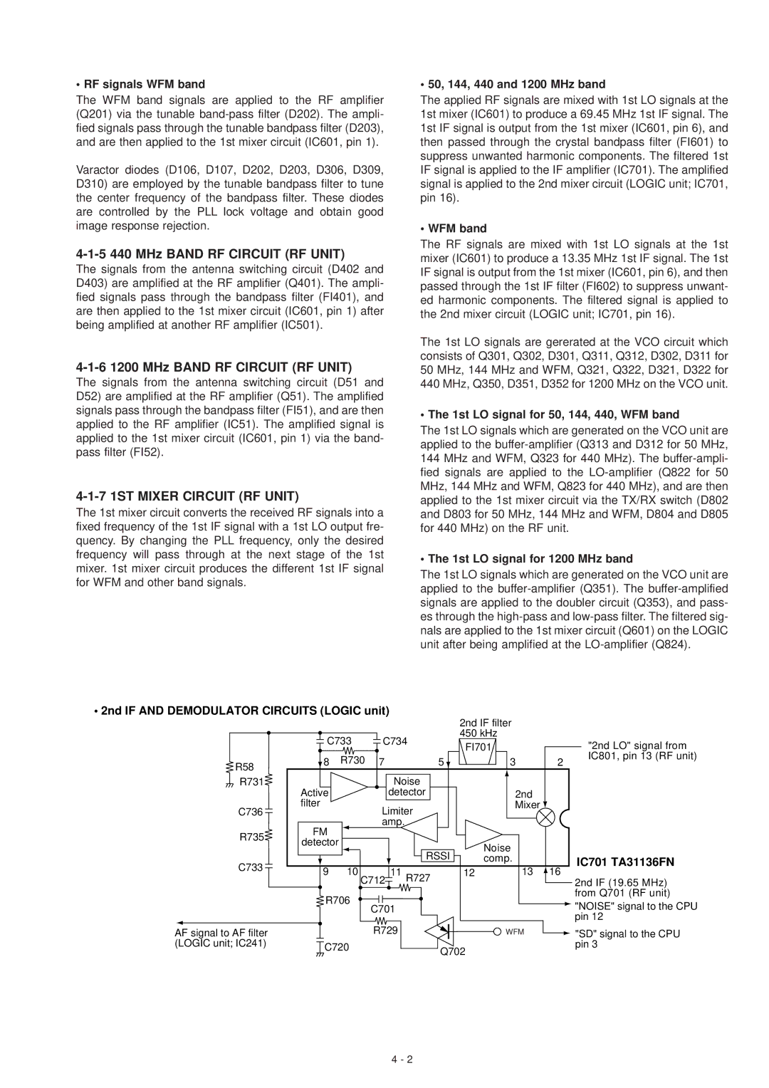
• 2nd IF AND DEMODULATOR CIRCUITS (LOGIC unit)
The applied RF signals are mixed with 1st LO signals at the 1st mixer (IC601) to produce a 69.45 MHz 1st IF signal. The 1st IF signal is output from the 1st mixer (IC601, pin 6), and then passed through the crystal bandpass filter (FI601) to suppress unwanted harmonic components. The filtered 1st IF signal is applied to the IF amplifier (IC701). The amplified signal is applied to the 2nd mixer circuit (LOGIC unit; IC701, pin 16).
• WFM band
The RF signals are mixed with 1st LO signals at the 1st mixer (IC601) to produce a 13.35 MHz 1st IF signal. The 1st IF signal is output from the 1st mixer (IC601, pin 6), and then passed through the 1st IF filter (FI602) to suppress unwant- ed harmonic components. The filtered signal is applied to the 2nd mixer circuit (LOGIC unit; IC701, pin 16).
The 1st LO signals are gererated at the VCO circuit which consists of Q301, Q302, D301, Q311, Q312, D302, D311 for 50 MHz, 144 MHz and WFM, Q321, Q322, D321, D322 for 440 MHz, Q350, D351, D352 for 1200 MHz on the VCO unit.
• The 1st LO signal for 50, 144, 440, WFM band
The 1st LO signals which are generated on the VCO unit are applied to the
• The 1st LO signal for 1200 MHz band
The 1st LO signals which are generated on the VCO unit are applied to the
R58
|
|
|
| 2nd IF filter |
C733 | C734 |
| 450 kHz | |
| FI701 | |||
|
|
|
| |
8 | R730 | 7 | 5 | 3 |
2
"2nd LO" signal from IC801, pin 13 (RF unit)
R731 | Noise |
Active | detector |
filter | Limiter |
C736 |
| amp. | |
R735 | FM | |
detector | ||
|
2nd Mixer ![]()
Noise |
C733
AF signal to AF filter (LOGIC unit; IC241)
9 | 10 C712 |
| RSSI |
|
|
|
| ||||
| 11 R727 | 12 | |||
|
|
|
| ||
R706
C701
R729
C720Q702
comp. | 16 | IC701 TA31136FN | |
13 | 2nd IF (19.65 MHz) | ||
|
|
| |
|
|
| from Q701 (RF unit) |
|
|
| "NOISE" signal to the CPU |
|
|
| |
|
|
| pin 12 |
WFM |
| "SD" signal to the CPU | |
| |||
|
|
| pin 3 |
4 - 2