Functional Description
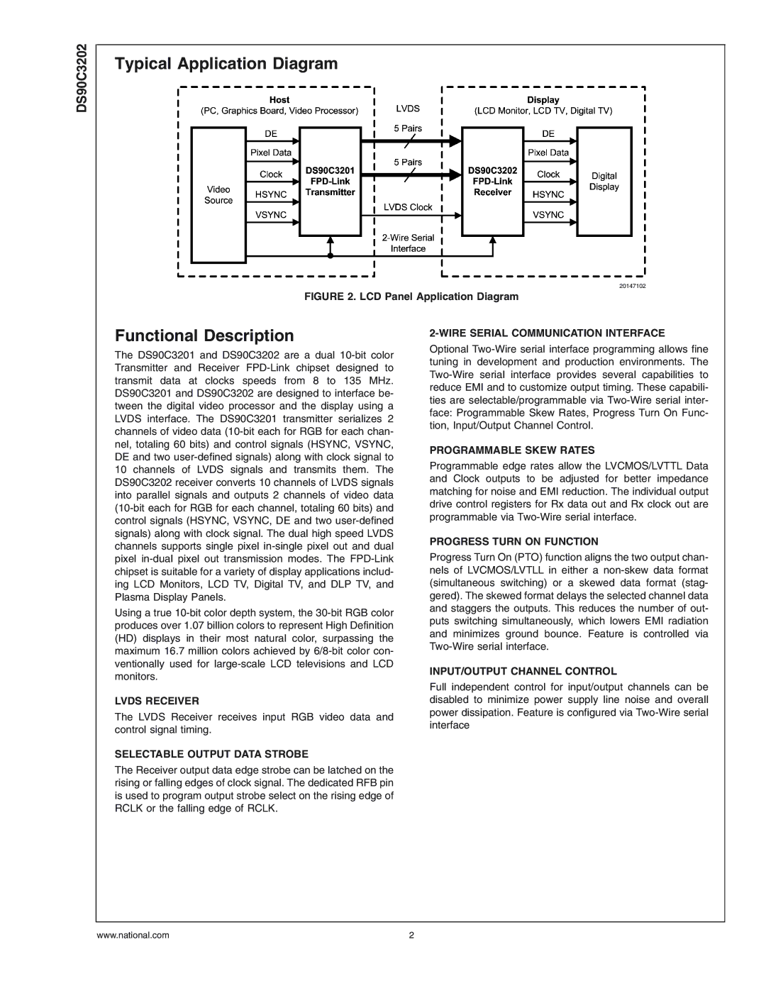
The DS90C3201 and DS90C3202 are a dual 10-bit color Transmitter and Receiver FPD-Link chipset designed to transmit data at clocks speeds from 8 to 135 MHz. DS90C3201 and DS90C3202 are designed to interface be- tween the digital video processor and the display using a LVDS interface. The DS90C3201 transmitter serializes 2 channels of video data (10-bit each for RGB for each chan- nel, totaling 60 bits) and control signals (HSYNC, VSYNC, DE and two user-defined signals) along with clock signal to 10 channels of LVDS signals and transmits them. The DS90C3202 receiver converts 10 channels of LVDS signals into parallel signals and outputs 2 channels of video data (10-bit each for RGB for each channel, totaling 60 bits) and control signals (HSYNC, VSYNC, DE and two user-defined signals) along with clock signal. The dual high speed LVDS channels supports single pixel in-single pixel out and dual pixel in-dual pixel out transmission modes. The FPD-Link chipset is suitable for a variety of display applications includ- ing LCD Monitors, LCD TV, Digital TV, and DLP TV, and Plasma Display Panels.
Using a true 10-bit color depth system, the 30-bit RGB color produces over 1.07 billion colors to represent High Definition (HD) displays in their most natural color, surpassing the maximum 16.7 million colors achieved by 6/8-bit color con- ventionally used for large-scale LCD televisions and LCD monitors.
LVDS RECEIVER
The LVDS Receiver receives input RGB video data and control signal timing.
SELECTABLE OUTPUT DATA STROBE
The Receiver output data edge strobe can be latched on the rising or falling edges of clock signal. The dedicated RFB pin is used to program output strobe select on the rising edge of RCLK or the falling edge of RCLK.
2-WIRE SERIAL COMMUNICATION INTERFACE
Optional Two-Wire serial interface programming allows fine tuning in development and production environments. The Two-Wire serial interface provides several capabilities to reduce EMI and to customize output timing. These capabili- ties are selectable/programmable via Two-Wire serial inter- face: Programmable Skew Rates, Progress Turn On Func- tion, Input/Output Channel Control.
PROGRAMMABLE SKEW RATES
Programmable edge rates allow the LVCMOS/LVTTL Data and Clock outputs to be adjusted for better impedance matching for noise and EMI reduction. The individual output drive control registers for Rx data out and Rx clock out are programmable via Two-Wire serial interface.
PROGRESS TURN ON FUNCTION
Progress Turn On (PTO) function aligns the two output chan- nels of LVCMOS/LVTLL in either a non-skew data format (simultaneous switching) or a skewed data format (stag- gered). The skewed format delays the selected channel data and staggers the outputs. This reduces the number of out- puts switching simultaneously, which lowers EMI radiation and minimizes ground bounce. Feature is controlled via Two-Wire serial interface.
INPUT/OUTPUT CHANNEL CONTROL
Full independent control for input/output channels can be disabled to minimize power supply line noise and overall power dissipation. Feature is configured via Two-Wire serial interface