MN101C115/117 LSI User’s Manual
Pub. No -011E
Page
Page
How to Read This Manual
Under plannin Unit Byte
Precautions and warnings
Subtitle Sub-subtitle
Main text Key information
Summary
Finding Desired Information
Page
Page
Contents0
Contents
Port Functions
Serial Functions
Appendices
Page
Chapter Overview
Product Overview
Overview
Product Summary
Model ROM Size RAM Size Classification
Hardware Functions
LED driver function 8 pins Ports
Operation modes Normal mode
Pins
Pin Diagram
MN101C117/115
MN101C117/115
Pin Function Summary
Pin No Name Type
Function Description
1 Pin Function Summary 2/4
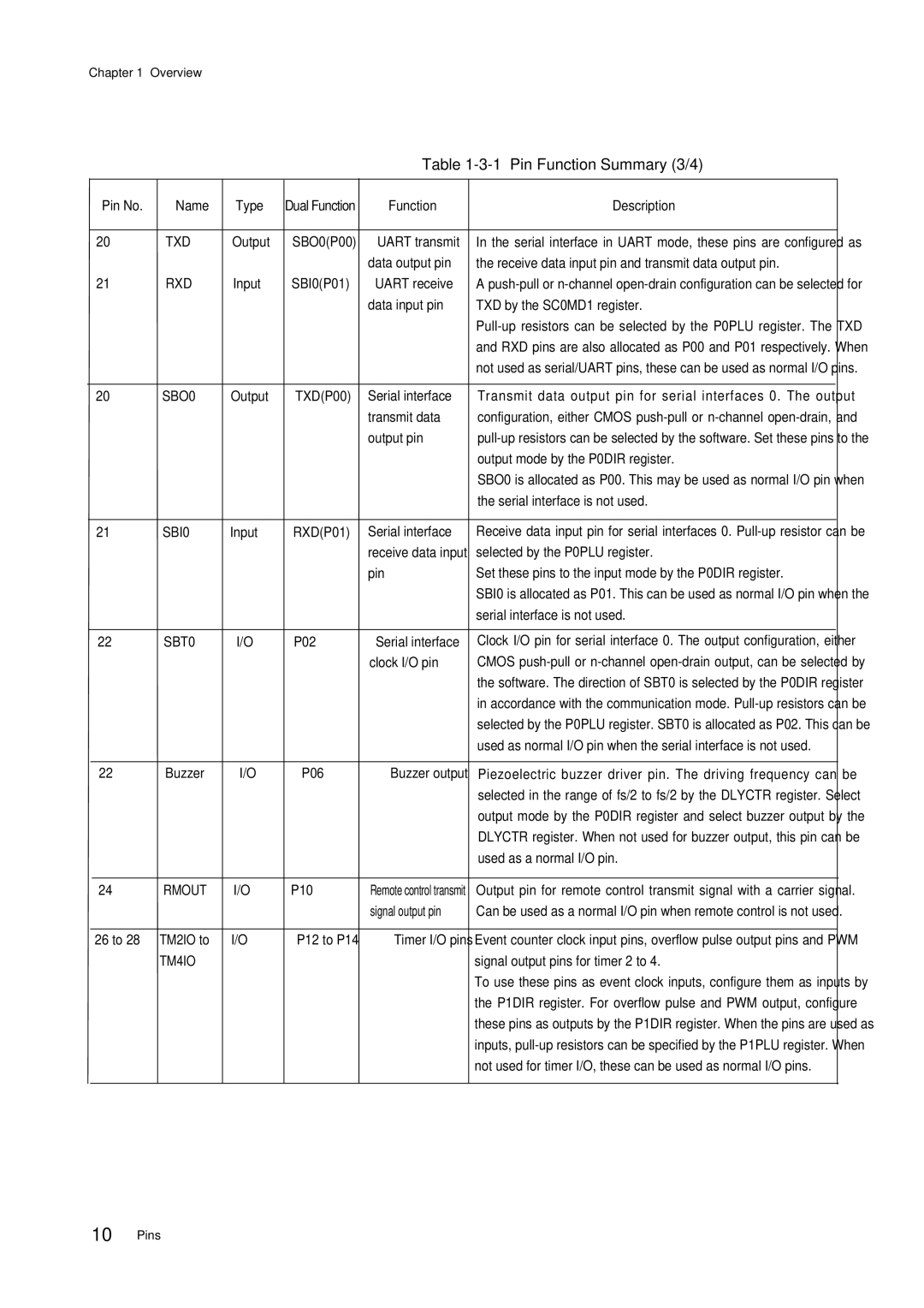
Rmout
1 Pin Function Summary 3/4
TXD
1 Pin Function Summary 4/4
Mmod
Block Diagram
Bit timer Conversion
Overview of Functions
MN101C00
Electrical Characteristics
Contents Model MN101C117/115
Parameter Symbol Rating Unit
Absolute Maximum Ratings ∗2 ∗3
Operating Conditions
Supply voltage
Operating speed ∗
Crystal oscillator 1 Fig
External clock input 1 OSC1 OSC2 is unconnected
External clock input 2 XI XO is unconnected*2
9VDD 1VDD Twh1twl1 Twr1twf1
DC Characteristics
Supply current no load at output ∗
Input pin 3-2 P21 when used as Sens
Input pin 1 Mmod
Input pin 2 P20, P22~P23 Schmitt trigger input
Input pin 3-1 P21 Schmitt trigger input
Sens pin
Input pin 4 PA0~PA7
Pin 5 P27 RST
Pin 6 P00 to P06, P10 to P14 Schmitt trigger input
Pin 7 , P60 to P67
Pin 8 P70 to P71
4 A/D Converter Characteristics
Pin 9 P80~P87
Option
ROM Option
Option Form
Model Name MN101C Date SE No Customer
Outline Drawings
Package code SDIP042-P-0600 Unit mm
Package code QFP044-P-1010 Unit mm
2 44-QFP
Package code QFH048-P-0707 Unit mm
3 48-QFH
Basic CPU Functions
Memory Configuration
Overview
Address Space
Special Function Registers
03FAX 03FBX 03FCX
03FDX 03FEX
03FFX
Bus Interface
Control Registers
Memory control registerMEMCTR
Memctr
Interrupts
Accepting and Returning from Interrupts
New SP
Low Address High
Operation when Returning from Interrupt
Interrupt Sources and Vector Addresses
Interrupt Control Registers
Non-maskable Interrupt Control Register Nmicr
XxxLV1 XxxLV0 XxxIE XxxIR At reset
Reset
Releasing the Reset
RST pin Clock cycles 200ns for a 20MHz oscillation
Chapter Port Functions
1 Status When Port Is Reset single-chip mode
Port 0 P0
2 Port 0 Functions
Port 1 P1
3 Port 1 Functions
Port 2 P2
4 Port 2 Functions
Port 7 P7
Port 7 Functions
Port 8 P8
Port 8 Functions
Port Control Registers
Name Address Function
Port Control Registers 2/2
At reset
At reset XXX
At reset Xxxxx
At reset 000
1 Port Control Registers 2/2
P7IN1 P7IN0 P8IN7 P8IN6 P8IN5 P8IN4 P8IN3 P8IN2 P8IN1 P8IN0
2 I/O Port Control Registers
Port Output/Input Mode Registers
O port Special function pin Pin Control Registers
I/O Port Configuration and Functions
P00,P02,P10 to P14
P01
P01 Pull-up Control bit
Resistor Register
Control Address
PA0 to PA7
PA0 PA1 PA2 PA3 PA4 PA5 PA6 PA7
Pin Configuration for P20, P22 to P23
P20 P22 P23 Pull-up Control bit
Port input Control bit
5 Configuration and Functions of P21
P21
6 Configuration and Functions of P27
P27
Configuration and Functions of P70
P70 to P71
P70 P71
Direction
8 Configuration and Functions of P60 to P67
P60 to P67,P80 to P87
Chapter Timer Functions
PWM output
Clock
Fs/4 Source
Fosc,fx/2
1 Timers 2, 3 Block Diagram
2 Timer 4 Block Diagram
3 Timer 5/Time Base Block Diagram
Wdirq
Wdctr
MUX
Dlyctr
5 Remote Control Transmission Block Diagram
Rmctr
8-bit Timer Operation timers 2
Bit
SIF0
Operation
1 Binary Counter 2 TM2BC Count Timing
64 8-bit Timer Operation timers 2
3 Timer Pulse Output Timing
Matches compare register Binary counter
4 PWM Output Timing
6 PWM Output Timing when TM2OC register is XFF
Clock PWM output
Disable the timer 2 interrupt
16-bit Timer Operation timer
1 Binary Counter 4 TM4BC Count Timing
Timer Functions
Matches TM4OCH, TM4OCL register Binary counter
4 Pulse Added Type PWM Output
Setting the Added Pulse Position
1 Pulse-Added PWM OutputFigure
Repeated 256 times FFPosition
Added pulse
Timer Functions
8-bit Timer Operation timer
Timer Operation
Base Time Settings TM5IR2 to
Time Base Operation
Clock Source
Watchdog Timer Operation
Setup and Operation
Remote Control Output Operation
1 Remote Control Carrier Output Waveform
Buzzer Output Setup and Operation
Buzzer Output
Timer Function Control Registers
Timer Control Registers
Name Address Function
Programmable Timer/Counters
TM2BC7 TM2BC6 TM2BC5 TM2BC4 TM2BC3 TM2BC2 TM2BC1 TM2BC0
TM3BC7 TM3BC6 TM3BC5 TM3BC4 TM3BC3 TM3BC2 TM3BC1 TM3BC0
Compare register 4 TM4OCL lower 8 bits
Binary Counter 4 TM4BCL X03F64, R
Binary Counter 4 TM4BCH X03F65, R
Binary counter 4 TM4BCH upper 8 bits
Input capture register TM4ICL lower 8 bits
Input Capture Register TM4ICL X03F66, R
TM5BC7 TM5BC6 TM5BC5 TM5BC4 TM5BC3 TM5BC2 TM5BC1 TM5BC0
Timer Mode Registers
TM2MD
TM2PWM
TM2EN
Timer 3 mode register TM3MD
TM3MD
TM3PWM
TM3EN
Timer 4 mode register TM4MD
TM4MD
IRQ0 IRQ1 IRQ2 TM4PWM
TM4EN
Timer 5 mode register TM5MD
TM5MD
TM5CK0
TM5IR0
Timer Control Registers
Watchdog timer control register Wdctr
Remote control carrier output control register Rmctr
Rmoen
Chapter Serial Functions
Serial Functions
1 Serial 0 Block Diagram
Synchronous Serial Interface
Serial Functions
SBT
SBO
SC0BSY
SBT SBO
Serial Functions
Start condition enabled Start condition disabled
Serial Interface Transfer Timing
1 Serial Data Input Edge and Output Edge serial interface
Receive Data Input Edge Transmit Data Output Edge
SBT0
SBI0
SBO0
Half-duplex Uart Serial Interface
1 Uart Transmission Timing
Reception
2 Uart Reception Timing
How to Use the Baud Rate Timer
Serial Interface Control Registers
SC0RXB
Transmit/Receive Shift Registers, Receive Data Buffer
Serial interface 0 transmit/receive shift register SC0TRB
SC0TRB
SC0RXB
Serial Interface Mode Registers
Serial interface 0 mode register SC0MD0
SC0MD0
SC0STE
Serial interface 0 mode register 1 SC0MD1
Serial interface 0 mode register 2 SC0MD2
SC0MD2
SC0NPE
SC0BRKE
Serial interface 0 mode register 3 SC0MD3
Serial Interface Control Register
Serial interface 0 control register SC0CTR
Chapter Conversion Functions
ANCTR0
AN0 AN1 AN2 AN3 AN4 AN5 AN6 AN7
ANCTR1 ANBUF1 ANBUF0
A/D Conversion
1 A/D Conversion Timing
2 Recommended Circuit When Using A/D Conversion
A/D Converter Control Registers
1 A/D Converter Control Registers
2 A/D Control Register Anctr
D control register 0 ANCTR0
AN0
D conversion control register 1 ANCTR1
ANCTR1 Anst
3 A/D Buffers Anbuf
5 4 3 2 1
Chapter AC Zero-Cross Circuit/Noise Filter
1 P21 Input Circuit Block Diagram
AC Zero-Cross Circuit Operation
1 AC Line Waveform and IRQ Generation Timing
1 Noise Filtering Circuit Block Diagram
Noise Filter
Example Input and Output Waveforms for Noise Filter
Sampling Input Waveform after noise filtering
AC Zero-Cross Control Register
Nfctr
Noise Filter Control Register Nfctr
Nfctr
NF0EN
128
Appendices8
Eprom Versions
Appendices
Appendices
Characteristics of Eprom Version
Operating temperature
Tion start control,runaway Internal ROM final address data
There are no other functional differences
Writing to Microcomputer with Internal Eprom
Fit in the writing adapter and position the No.1 pin
Vendor
Data I/O
Appendices
Option Bit
2 Option bitAddress X07FFF
Writing Adapter Connection
Package Code SDIP042-P-0600
Package code QFP044-P-1010 Pin pitch 8mm
4 MN101CP117-BLBCEPROM Writing Adapter Connections
Package code QFH048-P-0707 Pin pitch 5mm
5 MN101CP117-HP Eprom Writing Adapter connections
Instruction Set
1101 111a #16
∗1 d4 sign extended ∗2 d7 sign extended ∗3 d11 sign extended
0010 0011 0001 D11
0011 0100 0bp
Ver2.01997.9.26
Instruction Map
MN101C00 Series Instruction MAP
Cbeq #8,abs16,d7/11 Cbne #8,abs16,d7/11
Summary of Special Function Registers
Cpum
P6IN7
P2PLU2
TM2BC4 TM2BC3 TM2BC2 TM2BC1
Nmicr Wdir
TBLV0 Tbir
MN101C115
Matsushita Electronics Corporation
Sales Offices