PATTON ELECTRONICS CO. | 3040/V35 | INSTALLATION AND OPERATIONS MANUAL |
139001UA
Equipment Grounding
Switch
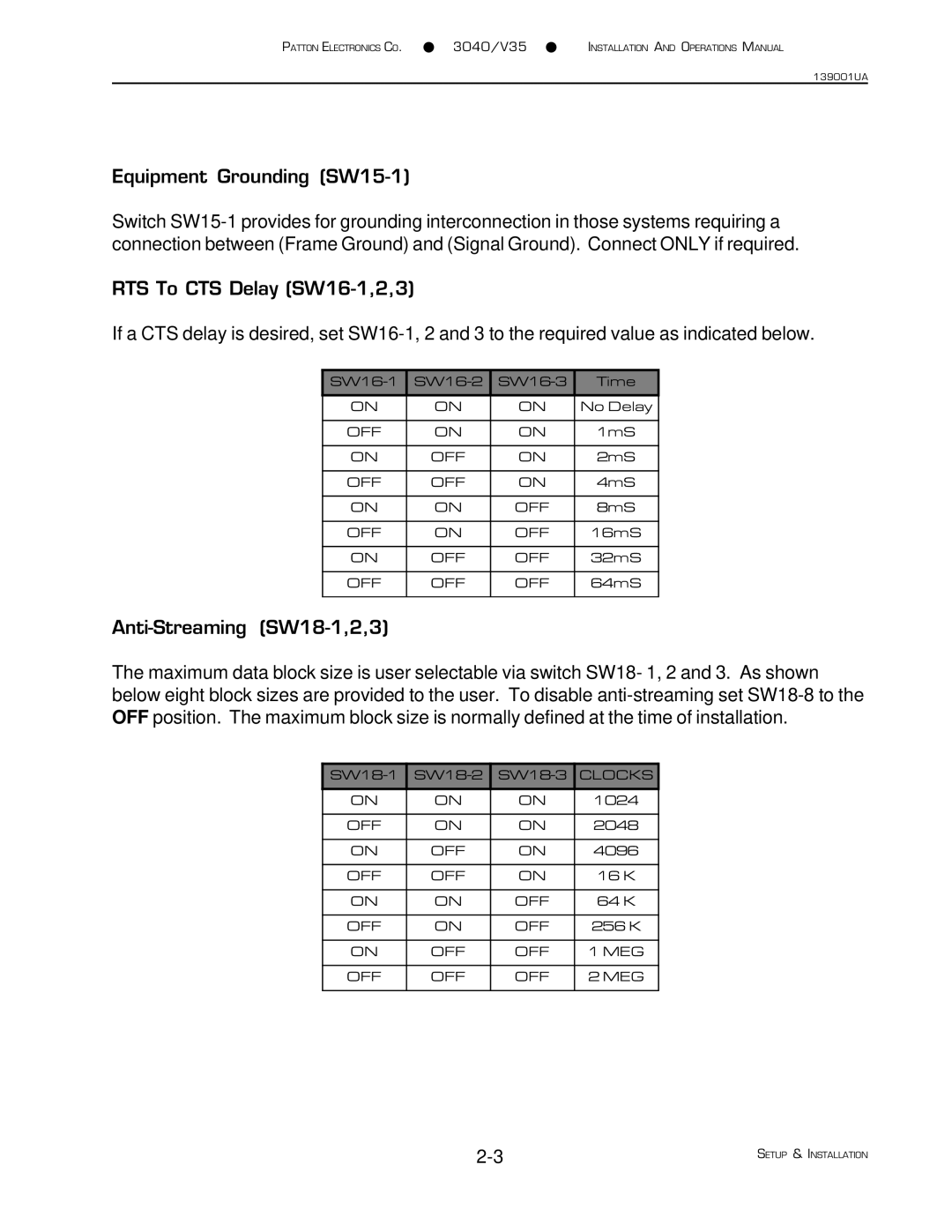
RTS To CTS Delay
If a CTS delay is desired, set
ON | ON | ON | No Delay |
|
|
|
|
OFF | ON | ON | 1mS |
|
|
|
|
ON | OFF | ON | 2mS |
|
|
|
|
OFF | OFF | ON | 4mS |
|
|
|
|
ON | ON | OFF | 8mS |
|
|
|
|
OFF | ON | OFF | 16mS |
|
|
|
|
ON | OFF | OFF | 32mS |
|
|
|
|
OFF | OFF | OFF | 64mS |
|
|
|
|
The maximum data block size is user selectable via switch SW18- 1, 2 and 3. As shown below eight block sizes are provided to the user. To disable
ON | ON | ON | 1024 |
|
|
|
|
OFF | ON | ON | 2048 |
|
|
|
|
ON | OFF | ON | 4096 |
|
|
|
|
OFF | OFF | ON | 16 K |
|
|
|
|
ON | ON | OFF | 64 K |
|
|
|
|
OFF | ON | OFF | 256 K |
|
|
|
|
ON | OFF | OFF | 1 MEG |
|
|
|
|
OFF | OFF | OFF | 2 MEG |
|
|
|
|
SETUP & INSTALLATION |