PATTON ELECTRONICS CO. | 3040/V35 | INSTALLATION AND OPERATIONS MANUAL |
139001UA
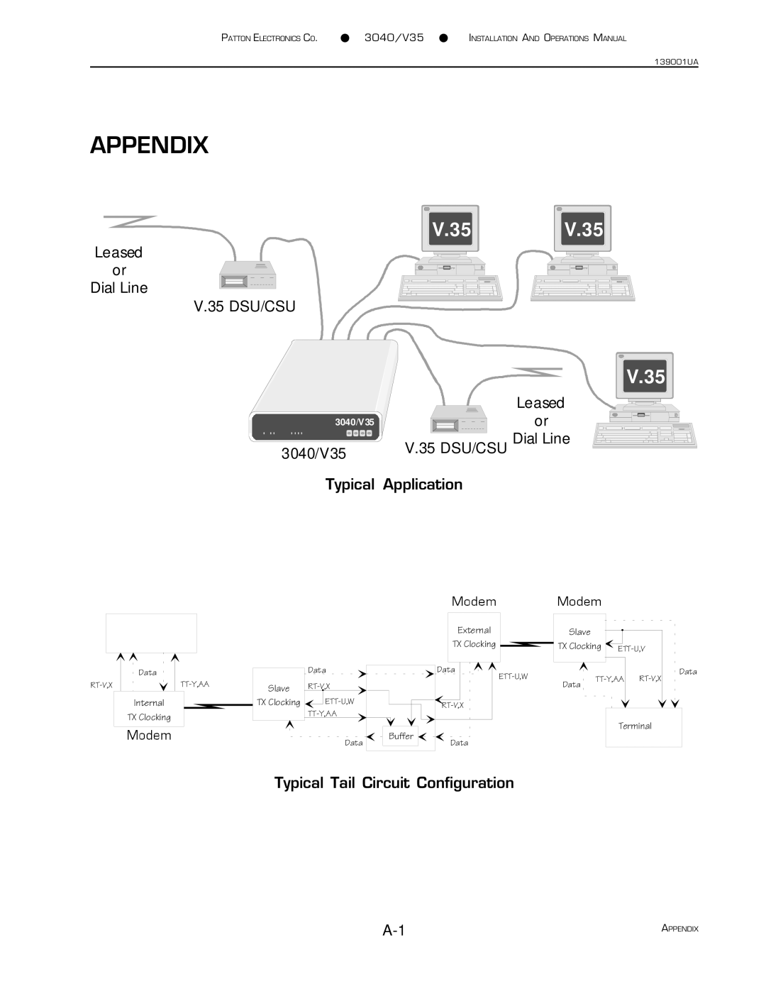
APPENDIX
V.35 | V.35 |
Leased |
|
or |
|
Dial Line |
|
V.35 DSU/CSU |
|
3040/V35
3040/V35
V.35
Leased |
or |
V.35 DSU/CSU Dial Line |
Typical Application
| Data |
Internal
TX Clocking
|
| External |
|
| TX Clocking |
| Data | Data |
|
| |
Slave |
| |
|
| |
TX Clocking | ||
| ||
|
| |
|
| Buffer |
| Data | Data |
Slave |
|
|
TX Clocking | ||
|
| Data |
Data |
|
|
| Terminal | |
Typical Tail Circuit Configuration
APPENDIX |