EN 6 |
| 2. |
| L06.1E | Safety Instructions, Warnings, and Notes |
semiconductors in the unit, irrespective of the type indication on these semiconductors.
•Manufactured under license from Dolby Laboratories. “Dolby”, “Pro Logic” and the
2.4.2Schematic Notes
•All resistor values are in ohms, and the value multiplier is often used to indicate the decimal point location (e.g. 2K2 indicates 2.2 kohm).
•Resistor values with no multiplier may be indicated with either an "E" or an "R" (e.g. 220E or 220R indicates 220 ohm).
•All capacitor values are given in
•Capacitor values may also use the value multiplier as the decimal point indication (e.g. 2p2 indicates 2.2 pF).
•An "asterisk" (*) indicates component usage varies. Refer to the diversity tables for the correct values.
•The correct component values are listed in the Spare Parts List. Therefore, always check this list when there is any doubt.
2.4.3Rework on BGA (Ball Grid Array) ICs
General
Although (LF)BGA assembly yields are very high, there may still be a requirement for component rework. By rework, we mean the process of removing the component from the PWB and replacing it with a new component. If an (LF)BGA is removed from a PWB, the solder balls of the component are deformed drastically so the removed (LF)BGA has to be discarded.
Device Removal
As is the case with any component that is being removed, it is essential when removing an (LF)BGA, that the board, tracks, solder lands, or surrounding components are not damaged. To remove an (LF)BGA, the board must be uniformly heated to a temperature close to the reflow soldering temperature. A uniform temperature reduces the risk of warping the PWB. To do this, we recommend that the board is heated until it is certain that all the joints are molten. Then carefully pull the component off the board with a vacuum nozzle. For the appropriate temperature profiles, see the IC data sheet.
Area Preparation
When the component has been removed, the vacant IC area must be cleaned before replacing the (LF)BGA.
Removing an IC often leaves varying amounts of solder on the mounting lands. This excessive solder can be removed with either a solder sucker or solder wick. The remaining flux can be removed with a brush and cleaning agent.
After the board is properly cleaned and inspected, apply flux on the solder lands and on the connection balls of the (LF)BGA. Note: Do not apply solder paste, as this has been shown to result in problems during
Device Replacement
The last step in the repair process is to solder the new component on the board. Ideally, the (LF)BGA should be aligned under a microscope or magnifying glass. If this is not possible, try to align the (LF)BGA with any board markers. So as not to damage neighbouring components, it may be necessary to reduce some temperatures and times.
More Information
For more information on how to handle BGA devices, visit this URL: www.atyourservice.ce.philips.com (needs subscription, not available for all regions). After login, select “Magazine”, then go to “Repair downloads”. Here you will find Information on how to deal with
2.4.4Lead-free Solder
Philips CE is producing
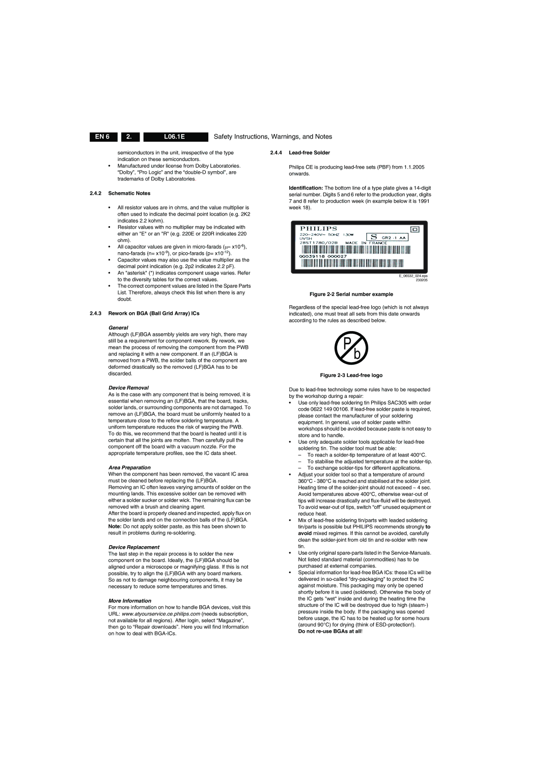
Identification: The bottom line of a type plate gives a
E_06532_024.eps 230205
Figure 2-2 Serial number example
Regardless of the special
Pb
Figure 2-3 Lead-free logo
Due to
•Use only
•Use only adequate solder tools applicable for
–To reach a
–To stabilise the adjusted temperature at the
–To exchange
•Adjust your solder tool so that a temperature of around 360°C - 380°C is reached and stabilised at the solder joint. Heating time of the
•Mix of
•Use only original
•Special information for
Do not