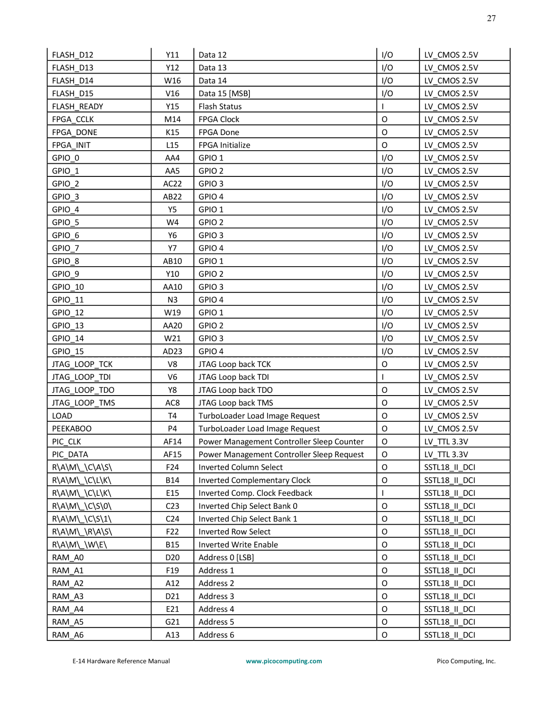
27


FLASH_D12


Y11


Data 12


I/O


LV_CMOS 2.5V


FLASH_D13


Y12


Data 13


I/O


LV_CMOS 2.5V


FLASH_D14


W16


Data 14


I/O


LV_CMOS 2.5V


FLASH_D15


V16


Data 15 [MSB]


I/O


LV_CMOS 2.5V


FLASH_READY


Y15


Flash Status


I


LV_CMOS 2.5V


FPGA_CCLK


M14


FPGA Clock


O


LV_CMOS 2.5V


FPGA_DONE


K15


FPGA Done


O


LV_CMOS 2.5V


FPGA_INIT


L15


FPGA Initialize


O


LV_CMOS 2.5V


GPIO_0


AA4


GPIO 1


I/O


LV_CMOS 2.5V


GPIO_1


AA5


GPIO 2


I/O


LV_CMOS 2.5V


GPIO_2


AC22


GPIO 3


I/O


LV_CMOS 2.5V


GPIO_3


AB22


GPIO 4


I/O


LV_CMOS 2.5V


GPIO_4


Y5


GPIO 1


I/O


LV_CMOS 2.5V


GPIO_5


W4


GPIO 2


I/O


LV_CMOS 2.5V


GPIO_6


Y6


GPIO 3


I/O


LV_CMOS 2.5V


GPIO_7


Y7


GPIO 4


I/O


LV_CMOS 2.5V


GPIO_8


AB10


GPIO 1


I/O


LV_CMOS 2.5V


GPIO_9


Y10


GPIO 2


I/O


LV_CMOS 2.5V


GPIO_10


AA10


GPIO 3


I/O


LV_CMOS 2.5V


GPIO_11


N3


GPIO 4


I/O


LV_CMOS 2.5V


GPIO_12


W19


GPIO 1


I/O


LV_CMOS 2.5V


GPIO_13


AA20


GPIO 2


I/O


LV_CMOS 2.5V


GPIO_14


W21


GPIO 3


I/O


LV_CMOS 2.5V


GPIO_15


AD23


GPIO 4


I/O


LV_CMOS 2.5V


JTAG_LOOP_TCK


V8


JTAG Loop back TCK


O


LV_CMOS 2.5V


JTAG_LOOP_TDI


V6


JTAG Loop back TDI


I


LV_CMOS 2.5V


JTAG_LOOP_TDO


Y8


JTAG Loop back TDO


O


LV_CMOS 2.5V


JTAG_LOOP_TMS


AC8


JTAG Loop back TMS


O


LV_CMOS 2.5V


LOAD


T4


TurboLoader Load Image Request


O


LV_CMOS 2.5V


PEEKABOO


P4


TurboLoader Load Image Request


O


LV_CMOS 2.5V


PIC_CLK


AF14


Power Management Controller Sleep Counter


O


LV_TTL 3.3V


PIC_DATA


AF15


Power Management Controller Sleep Request


O


LV_TTL 3.3V


R\A\M\_\C\A\S\


F24


Inverted Column Select


O


SSTL18_II_DCI


R\A\M\_\C\L\K\


B14


Inverted Complementary Clock


O


SSTL18_II_DCI


R\A\M\_\C\L\K\


E15


Inverted Comp. Clock Feedback


I


SSTL18_II_DCI


R\A\M\_\C\S\0\


C23


Inverted Chip Select Bank 0


O


SSTL18_II_DCI


R\A\M\_\C\S\1\


C24


Inverted Chip Select Bank 1


O


SSTL18_II_DCI


R\A\M\_\R\A\S\


F22


Inverted Row Select


O


SSTL18_II_DCI


R\A\M\_\W\E\


B15


Inverted Write Enable


O


SSTL18_II_DCI


RAM_A0


D20


Address 0 [LSB]


O


SSTL18_II_DCI


RAM_A1


F19


Address 1


O


SSTL18_II_DCI


RAM_A2


A12


Address 2


O


SSTL18_II_DCI


RAM_A3


D21


Address 3


O


SSTL18_II_DCI


RAM_A4


E21


Address 4


O


SSTL18_II_DCI


RAM_A5


G21


Address 5


O


SSTL18_II_DCI


RAM_A6


A13


Address 6


O


SSTL18_II_DCI


E‐14 Hardware Reference Manual


www.picocomputing.com


Pico Computing, Inc.

Page 27
Image 27
Pico Communications E-14 manual FLASHD12

E-14 specifications

Pico Communications E-14 is an advanced wireless communication device designed to meet the demands of modern connectivity. As a versatile solution, it serves various applications in sectors such as telecommunications, IoT, and smart cities. The E-14 stands out for its compact design, exceptional performance, and robust feature set that cater to both individual users and enterprises.

One of the primary features of the Pico E-14 is its support for multiple communication protocols, including LTE, NB-IoT, and LoRaWAN. This multi-protocol capability ensures that users can select the most suitable option for their specific use case, whether it be high-speed data transfer or low-power wide-area networking. With seamless integration into existing infrastructure, the E-14 facilitates hassle-free deployments.

Power efficiency is another hallmark of the Pico E-14. Designed for longevity, the device includes intelligent power management features that drastically reduce energy consumption, making it an ideal choice for battery-operated devices and remote monitoring applications. This capability is particularly valuable in settings where maintenance access is limited, and downtime must be minimized.

The E-14’s built-in security features provide enhanced data protection, making it suitable for applications that require confidentiality and integrity. With end-to-end encryption, secure boot, and trusted platform modules, users can rest assured that their data remains protected against unauthorized access and cyber threats.

Moreover, the Pico E-14 boasts a user-friendly interface, which simplifies setup and operation. Its intuitive configuration tools allow users to quickly adjust settings and monitor performance metrics, reducing the need for specialized technical knowledge. This ease of use is a significant advantage in environments where teams may vary in technical expertise.

The device is also rugged and built to withstand harsh environmental conditions. Its robust casing protects against dust, moisture, and extreme temperatures, allowing it to function reliably in a variety of settings, from urban installations to remote field deployments.

With its array of features, the Pico Communications E-14 is well-positioned to play a pivotal role in the evolution of connectivity solutions. By offering flexible communication methods, energy efficiency, enhanced security, and user-friendly functionality, it addresses the complexities of modern communication needs while paving the way for innovative applications in the future.