| M65881AFP |
|
|
|
|
|
|
|
|
|
|
|
| ||
| 3. System2 Mode |
|
|
|
|
|
|
| No setting bits means "Don't care". | ||||||
|
|
|
|
|
|
|
|
|
|
|
|
| |||
| bit | Flag name |
|
| Functional Explanation |
| H |
| L |
| INIT | ||||
1 | MODE1 |
| Mode settiing1 |
|
|
|
| "H" fixed |
|
|
|
| - | ||
2 | MODE2 |
| Mode setting2 |
|
|
|
|
|
| "L" fixed |
| - | |||
3 | IMCKSEL |
| Input master clock Selection |
| 512fsi |
| 256fsi |
| L | ||||||
4 |
|
|
|
|
|
|
|
|
|
|
|
|
| - | |
5 |
|
|
|
|
|
|
|
|
|
|
|
|
| - | |
6 | SYNC |
|
|
|
|
| L |
| L | ||||||
7 | XFsoOEN |
| XfsoOUT pin output "enable". |
| disable |
| enable |
| L | ||||||
8 | ASYNCEN2 | Asynchronous Detection Flag for secondary Side |
| enable |
| disable |
| L | |||||||
9 | CHSEL |
| L/R inversion of PWM output pin |
| active |
|
| L | |||||||
10 | DRPOL |
| ΔΣ Block : Rch Input Phase |
| Negative phase | Positive phase |
| L | |||||||
11 | SRCRST |
| Sampling Rate Converter Reset |
| active |
|
| L | |||||||
12 | CHRSEL |
| L/R inversion of PWM output pin |
| active |
|
| L | |||||||
13 | GIMUTE |
| Zero Mute at Gain Control Input Clock |
| active |
|
| L | |||||||
14 | NSPMUTE |
| Duty 50% Mute for PWM Output |
| active |
|
| L | |||||||
15 | PGMUTE |
| G_MUTE of PWM Output Data |
| active |
|
| L | |||||||
16 | NSSPEED |
| ΔΣ Block : Operating Speed |
| 32fso |
| 16fso |
| L | ||||||
17 | NSOBIT |
| ΔΣ Block : Setting of Output bit number |
| 5bit (31value) | 6bit (63 value) |
| L | |||||||
18 | DCDRPOL |
| ΔΣ Block : Rch Phase of AC dithering |
| Negative phase | Positive phase |
| L | |||||||
19 | DCDSEL0 |
|
| ΔΣ Block : DC dithering selection |
| Refer to Table |
|
| L | ||||||
20 | DCDSEL1 |
|
|
|
| L | |||||||||
|
|
|
|
|
|
|
|
|
|
|
| ||||
21 | ACDRPOL |
| ΔΣ Block : Rch Phase of AC dithering |
| Negative phase | Positive phase |
| L | |||||||
22 | ACDSEL0 |
|
|
|
|
|
|
|
|
|
|
|
| L | |
23 | ACDSEL1 |
|
| ΔΣ Block : AC dithering selection |
| Refer to Table |
| L | |||||||
24 | ACDSEL2 |
|
|
|
|
|
|
|
|
|
|
|
| L | |
| Table |
|
|
|
|
|
|
| |||||||
| bit | Flag name | Non dithering | DC dithering 0.1% |
| DC dithering 0.2% | DC dithering 0.4% |
|
| ||||||
19 | DCDSEL0 |
| L |
| H |
|
| L |
| H |
|
| |||
20 | DCDSEL1 |
| L |
| L |
|
| H |
| H |
|
| |||
| Table |
|
|
|
|
|
|
| |||||||
| bit | Flag name |
| Non dithering | AC dithering A |
|
| AC dithering C | AC dithering E |
|
| ||||
| 22 | ACDSEL0 |
| don't care |
| L |
|
| L |
| L |
|
| ||
| 23 | ACDSEL1 |
| L |
| H |
|
| L |
| H |
|
| ||
| 24 | ACDSEL2 |
| L |
| L |
|
| H |
| H |
|
| ||
| Table |
|
|
|
|
|
|
|
|
|
| ||||
| bit | Flag / Pin code name | 16fso,6bit |
| 16fso,5bit |
| 16fso, 5bit |
| 32fso, 5bit |
| |||||
| 16 | NSSPEED |
| L |
| L |
| X |
| H |
| ||||
| 17 | NSOBIT |
| L |
| H |
| X |
| H |
| ||||
| Pin | MCKSEL |
| L |
| L |
| H |
| L |
| ||||
|
| ( Secondary master clock | ( Secondary master |
| ( Secondary master clock | ( Secondary master |
| ||||||||
|
|
|
|
| 1024fso) |
| clock 1024fso) |
| 512fso) |
| clock 1024fso) |
| |||
|
|
|
|
|
|
|
|
|
|
|
|
|
|
|
|
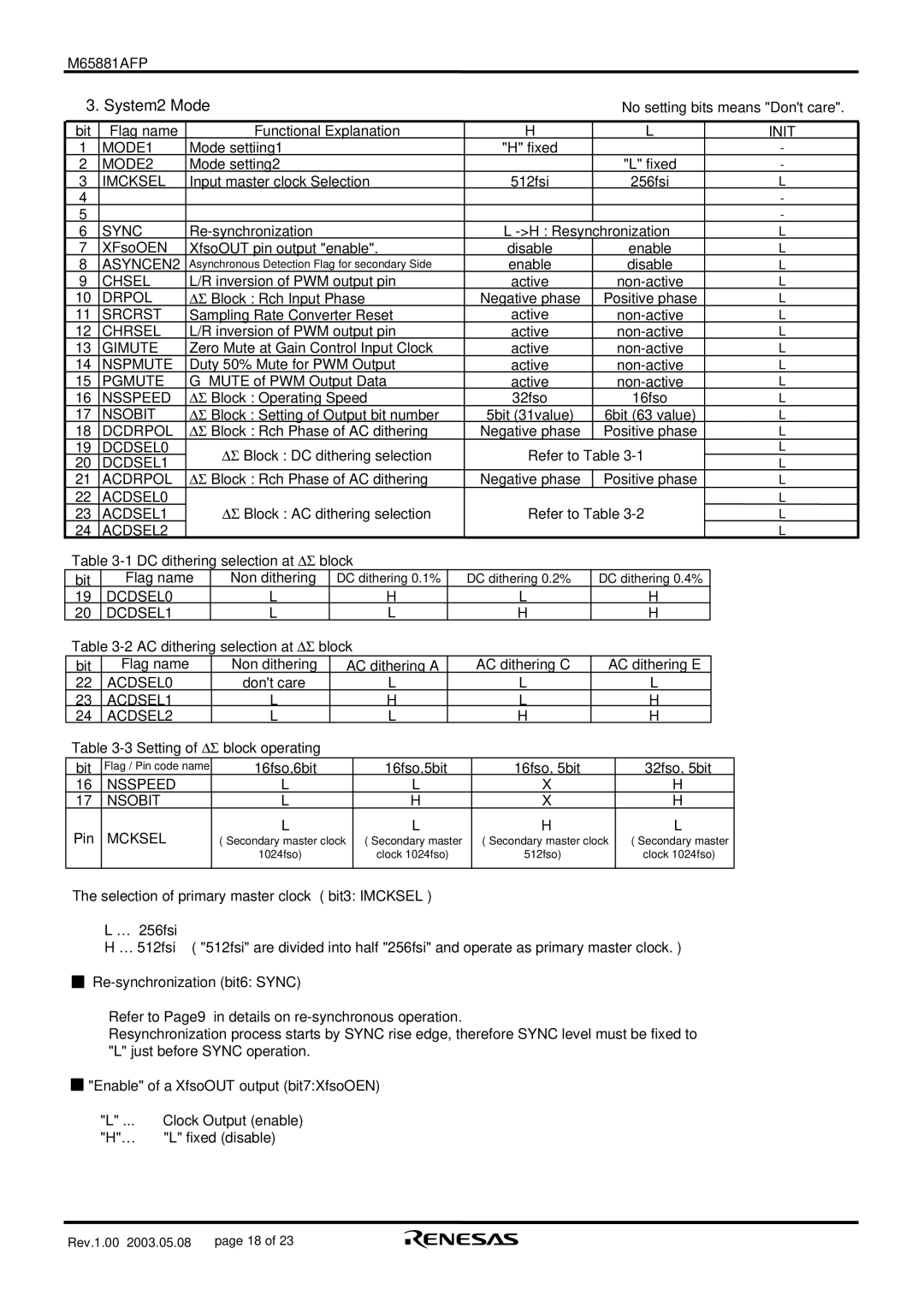
The selection of primary master clock ( bit3: IMCKSEL )
L … 256fsi
H … 512fsi ( "512fsi" are divided into half "256fsi" and operate as primary master clock. )
Refer to Page9 in details on
Resynchronization process starts by SYNC rise edge, therefore SYNC level must be fixed to "L" just before SYNC operation.
![]()
![]() "Enable" of a XfsoOUT output (bit7:XfsoOEN)
"Enable" of a XfsoOUT output (bit7:XfsoOEN)
"L" ... | Clock Output (enable) |
"H"… | "L" fixed (disable) |
Rev.1.00 2003.05.08 | page 18 of 23 |
