Manuals
/
Silicon Laboratories
/
Household Appliance
/
Home Security System
Silicon Laboratories
SI4421 Si4421, Description of the Control Commands, Power Management Command
Models:
SI4421
1
15
45
45
Download
45 pages
20.88 Kb
12
13
14
15
16
17
18
19
Specification
AC Characteristics Receiver
Functional Block Diagram
Wake-UpTimer
FIFO and Reset Mode Command
Control Commands
Configuration Setting Command
RF Power Amplifier PA
Page 15
Image 15
Page 14
Page 16
Page 15
Image 15
Page 14
Page 16
Contents
TYPICAL APPLICATIONS
FUNCTIONAL BLOCK DIAGRAM
FEATURES
DESCRIPTION
Si4421
DETAILED FEATURE-LEVELDESCRIPTION
RF Power Amplifier PA
Data Filtering and Clock Recovery
Crystal Oscillator
Low Battery Voltage Detector
Wake-UpTimer
Data Validity Blocks
Function
Si4421 PACKAGE PIN DEFINITIONS
Name
Type
Internal connection
Si4421
Internal Pin Connections
Name
Si4421
PIN6 Logic Diagram FSK / DATA / nFFS
PIN10 Logic Diagram nRES I/O
Note These pins can be left floating
Pin Function vs. Operation Mode
Si4421
Typical Application
Recommended supply decoupling capacitor values
Si4421 GENERAL DEVICE SPECIFICATIONS
Absolute Maximum Ratings non-operating
Recommended Operating Range
ELECTRICAL SPECIFICATION
DC Characteristics
Si4421
AC Characteristics PLL parameters
AC Characteristics Receiver
Si4421
AC Characteristics Others
Si4421
AC Characteristics Transmitter
AC Characteristics Turn-on/Turnaroundtimings
Note 10 By design
Si4421
Si4421 CONTROL INTERFACE
Timing Specification
Timing Diagram
Control Commands
Control Register Default Values
Si4421
Si4421
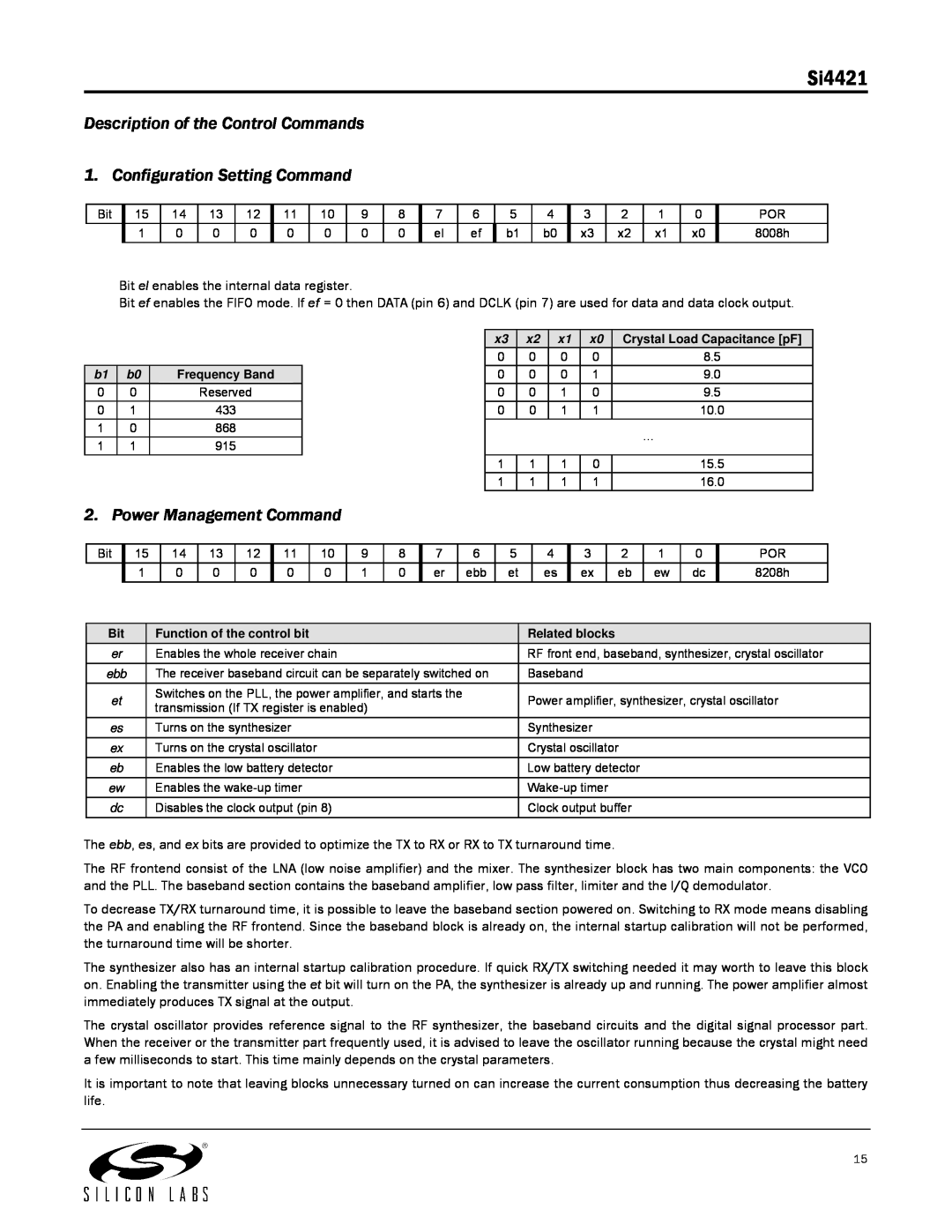
Description of the Control Commands
Configuration Setting Command
2. Power Management Command
Si4421
Logic connections between power control bits
Si4421
Frequency Setting Command
4. Data Rate Command
5. Receiver Control Command
Si4421
VDI Logic Diagram
Si4421
6. Data Filter Command
Si4421
7.FIFO and Reset Mode Command
Si4421
8. Synchron Pattern Command
9. Receiver FIFO Read Command
10. AFC Command
Bit 5-4rl1 to rl0
Si4421
11. TX Configuration Control Command
Frequency Setting Command
Si4421
13. Transmitter Register Write Command
12. PLL Setting Command
Si4421
14. Wake-UpTimer Command
15.Low Duty-CycleCommand
Si4421
Si4421
Vlb= 2.25 + V · 0.1 V Clock divider configuration
17. Status Read Command
Si4421
Bit Name
Si4421 INTERRUPT HANDLING
Si4421
TX REGISTER BUFFERED DATA TRANSMISSION
Typical TX register usage
Si4421
RECOMMENDED PACKET STRUCTURES
Si4421 RX FIFO BUFFERED DATA READ
Bit Rate 38.4 kbps
Si4421 CRYSTAL SELECTION GUIDELINES
Bit Rate 2.4 kbps
Bit Rate 9.6 kbps
Si4421 RX-TXALIGNMENT PROCEDURES
Si4421 RESET MODES
Si4421
Sensitive Reset Enabled, Ripple on Vdd
FIFO and Reset Mode Command page
SW Reset Command
Channel Selectivity and Blocking
Si4421 TYPICAL PERFORMANCE CHARACTERISTICS
Si4421
BER Curves in 433 MHz Band
BER Curves in 868 MHz Band
434 MHz
Si4421
Frequency Dependent Component Values
Si4421 REFERENCE DESIGNS
Schematics
Evaluation Board with 50 Ohm Matching Network
PCB Layout Top View Bottom View
Si4421
Frequency Dependent Component Values
Schematics
Si4421
Evaluation Board with Resonant PCB Antenna BIFA
Si4421
PCB Layout Antenna designed for 868/915 MHz band
Top View Bottom View
Si4421 PACKAGE INFORMATION
16-pinTSSOP
See Detail “A” Section B-B
Related Resources
RELATED PRODUCTS AND DOCUMENTS
Si4421 Universal ISM Band FSK Transceiver
Demo Boards and Development Kits
Si4421
Top
Page
Image
Contents