BPX-5
889-770-01
KEM-460AAA
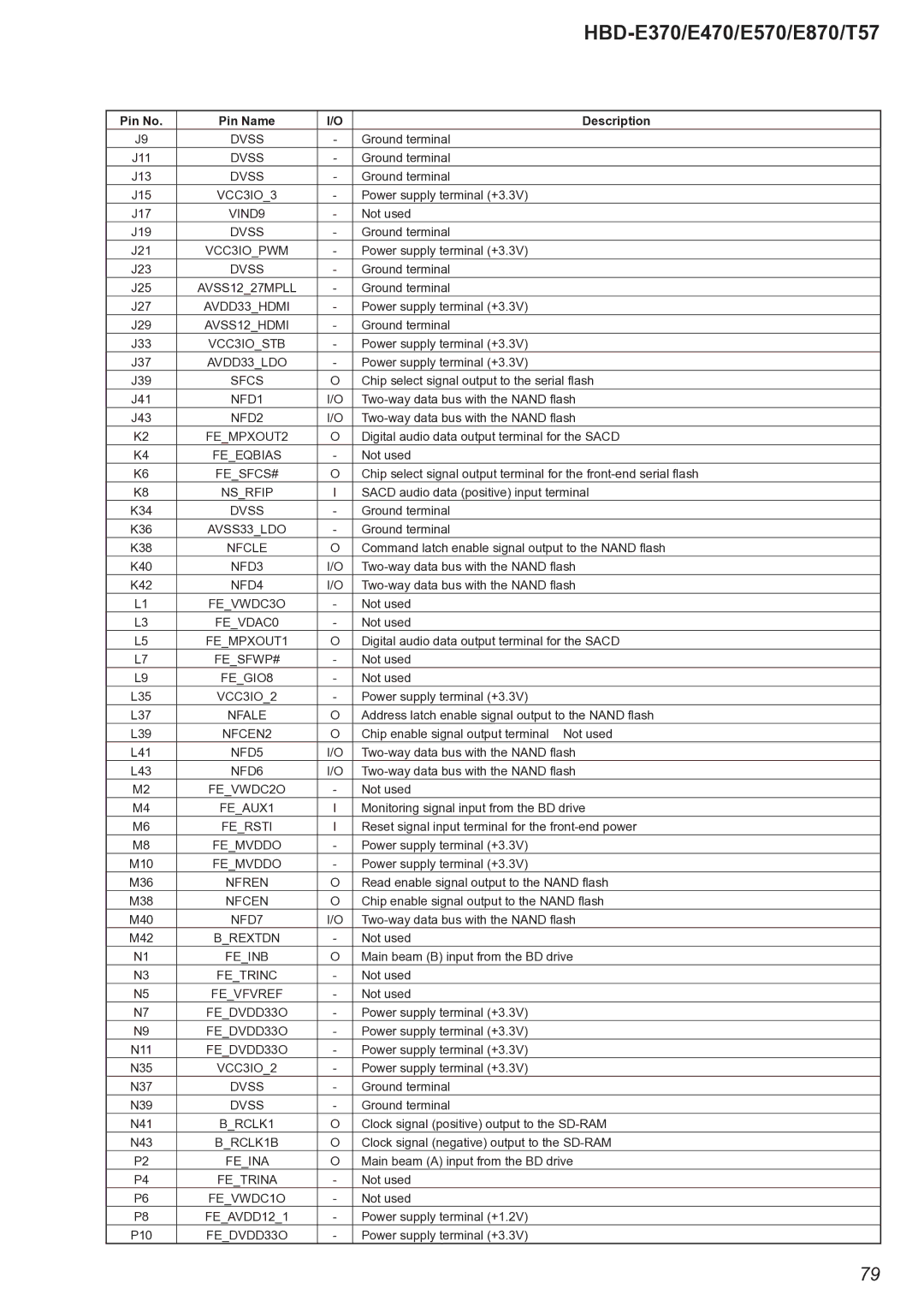
HBD-E370/E470/E570/E870/T57
Exploded Views
Table of Contents
Disassembly
Diagrams
CD HLX-A1 Procedure
Releasing Procedure
Operation and Display BLX-104 Procedure
BLX-204 Procedure
Barcode decoder Bdbudec Part No. J-6090-212-A
Install procedure
Preparation ESD Countermeasure
Jig
Flow of drive section check
Pass-fail judgment of the optical device KEM-460AAA
Flow of optical device IOP check
Specification value
Optical device KEM-460AAA replacement Flow of replacement
Rear Chassis
Chuck Holder Assy Loading Assy HOLDER, FFC Rear
Power Board Component Side
HOW to Open the Tray When Power Switch Turn OFF
Case EZ
Disassembly Flow
MB-134 Board
Bracket MB Block
Fuse F901, Power Board
Connect Board
Front Panel Block
Back Panel Block
BD Drive BPX-5
Audio Board
Main Board
Optical Device KEM-460AAA, Wire Flat Type
Main Functions
Setting method of the BD service mode
‡�LDJ�7HVW
Menu Tree
Operation
Service Mode Menu Top Menu
Screen 1 When video test category is selected Operation
Screen 2 When audio test category is selected Operation
Diag Audio Input Test
Log Error Log Output of each Log
Screen 2 Displays the Error Log Operation
Diag Wireless LAN Test
Screen 1 Ifconfig Test Operation
Factory Initialize Factory Settings
Operation Screen
Network Network Test Diagnosis Screen Ifconfig
Screen 3 Ping Test Active
Contents List
Network Network Test Diagnosis Screen Ping
Screen 1 Ping Test Operation
Screen 3 *Drive OP data Write
Screen 1 Selecting items under *Service Menu
Screen 5 *Servo Signal Check Menu Not Used
Drive
Screen 10 *Load Eject Aging Not Used
Screen 6 *S-Curve Check Menu Not Used
Screen 7 *Readability Check Menu Not Used
Screen 9 *OP Check Menu
Networking Confirmation
Screen 12 *FA Mode Test Not Used
Playback Operation Confirmation 1-1. Test Disc
Playback operation confirmation
Section Electrical Check
Block Diagram Servo Section
Section Diagrams
F42 Sfdo H40 Sfdi G41 Sfck J39 Sfcs Hold
Block Diagram Memory Section
5FK
Block Diagram TUNER, S-AIR Section
Block Diagram Audio Section
Block Diagram Regulator Section
31 H
Block Diagram PANEL, Power Supply Section
For Schematic Diagrams
Circuit Boards Location For Printed Wiring Boards
See page 77 for IC Pin Function Description
Schematic Diagram MB-134 Board 1/13
IC204 IC205
Schematic Diagram MB-134 Board 2/13
See page 67 for IC Block Diagrams
Schematic Diagram MB-134 Board 3/13
MB-134 Board
Schematic Diagram MB-134 Board 4/13
IC501
Schematic Diagram MB-134 Board 5/13
MB-134 Board
Schematic Diagram MB-134 Board 6/13
IC705
Schematic Diagram MB-134 Board 7/13
MB-134 Board
Schematic Diagram MB-134 Board 8/13
IC1003
Schematic Diagram MB-134 Board 9/13
10/13
11/13
Schematic Diagram MB-134 Board 11/13
MB-134 Board 12/13
13/13
Schematic Diagram MB-134 Board 13/13
IC502
Uses unleaded solder
IC601
Audio Board
Audio Board
Schematic Diagram Audio Board
Main Board
IC700
Main Board 1/5
Main Board
Schematic Diagram Main Board 2/5
Main Board
See page 60 for waveforms See page 67 for IC Block Diagrams
Schematic Diagram Main Board 4/5
IC700
Schematic Diagram Connect Board
Printed Wiring Board Connect Board
Waveforms Main Board
Printed Wiring Board REG Board
IC400
Schematic Diagram REG Board
IC803
FL Board
Schematic Diagram FL Board
Power Board
Power Board
Schematic Diagram Power Board
Schematic Diagram KEY Section
Printed Wiring Boards KEY Section
IC308 MP2301ENE-LF-Z
IC Block Diagrams MB-134 Board
IC601, 602 SI-3010KM-TLS
IC2301 TPIC1391DBTRG4
IC2401 TPIC1405DFDRG4
IC702 PCM1808PWR
Audio Board
IC703 LC89058W-E
IC3011 SI-3010KM-TLS
FL Board
REG Board
IC921 STR-Y6763 IC941 SI-3010KM-TLS
Power Board
VOUTD9
Fesfdo
VOUTD1
VOUTD5
Clkp
Mreset
Reset
CH1P
Tnpllg
VIND7
Mcin
AVSS12DMPLL
NFD1
VIND9
VCC3IOPWM
Sfcs
Feing
NFRBN2
Nfrbn
VCC2IO
BRDQS2
Vcckpwm
BRDQ18
BRDQ21
AC9 FEDVDD33O
AC3 FELVDS3P
AC5 FELVDS5P
AC7 FEAVDD124
FEFMO3
FEGIO3
Felimit
FEGAINSW3
FESVDD33
AP4 Coreresetb
USBDP0
USBDM1
Arvref
ARDQ5
ARDQM0
ARDQ11
Arodt
GPIO5
ARDQ1
ARDQ12
BB8 XTAL25MI
BB2 SRXN1
BB4 SRXN2
BB6 Svctst
Mdio
Txer
MDC
CRS
Dircl
Bdreset
DAMPSCDT/DIRDI
Dampshift
Pvdddet
Micdet
Dcdet
Driversd
Escutcheon EZ E870
KNOB, Balance White . . . RED
Panel Front Assy 10EZ
Escutcheon EZ E570
MB-134 Board Section
Tuner FM AEP, UK
Back Panel Section
DC FAN TU1
Tuner FM US, CND TU1
Main Board Section
BD Drive Section BPX-5
202 A-1750-926-A Loading for Service
Audio
Audio Connect
FL F-USB KEY Main
Film
Main
Ceramic Chip 7PF
Ceramic Chip 4PF
PIN, Connector Small Type 2P Diode
CONNECTOR, FFC/FPC 27P
CONNECTOR, FFC/FPC 15P
CONNECTOR, FFC/FPC 16P
AIR-CORE Coil Transistor
AIR-CORE Coil
Transistor RT3CLLM
102
Terminal
MB-134
Vibrator
104
Elect Chip
Diode KDZTR3.9B
Ethernet Connector 8P LAN
CONNECTOR, FFC/FPC ZIF 45P
Common Mode Choke Coil
Transistor FDC642P
Contact Terminal
FET
108
MB-134 P-KEY Power
Power
Power REG
REG R-USB
Memo
Ver Date Description of Revision
Revision History