MDM-7X2A
Specifications
MD Section
HCD-PX333 SELF-DIAGNOSIS Function
HCD-PX333
Items of Error History Mode Items and Contents
Error Code Details of Error
Table of Error Codes
CD Section
Model Identification
Table of Contents
Electrical Adjustments
Diagrams
For MD
Cleaning Objective Lens of Optical PICK-UP
HCD-PX333 Section Servicing Notes
For CD
Service Position
IOP
JIG for Checking BD MD Board Waveform
Record Procedure
When Memory NG is Displayed
Criteria for Determination Measure if unsatisfactory
Checks Prior to Parts Replacement and Adjustments in MD
Specified Value
Bit Binary
Retry Cause Display Mode in MD
Higher Bits Lower Bits Hexa Details
Decimal Bit When Binary
Hexadecimal Binary
CD aging mode sequence
CD Aging Mode
Checking Method
CD-TEXT Test Disc
Restrictions in CD-TEXT Display
CD-TEXT Test Disc Recorded Contents and Display
Section General HCD-PX333
Parts Identification
Remote Control
This set can be disassembled in the order shown below
HCD-PX333 Section Disassembly
Front Panel Section
Case
REC BOARD, VOL Board
Jack BOARD, BL BOARD, Panel BOARD, LCD
Back PANEL, SP BOARD, Tuner
TRANSFORMER, Power and DC FAN
AMP Board
Main BOARD, Power Board
Over Write Head HR901, BD MD Board
MD Mechanism Deck MDM-7X2A
Loading Motor Assy M103
Holder Assy
Optical PICK-UP KMS-262
Sled Motor Assy M102
CD Mechanism Deck CDM55A-21BD53
Spindle Motor Assy M101
Holder BU Assy
MD Digital Board
Tray CDM, Loading Board
Base Unit BU-21BD53, Holder 55-BU21
CAM CDM55
HCD-PX333 Section Test Mode
Basic Operations of the Test Mode
MD Seciton Precautions for USE of Test Mode
Setting the Test Mode
Releasing the Test Mode
Check
Selecting the Test Mode
OUT
Operating the Continuous Playback Mode
Functions of Other Buttons
MID
Meanings of Other Displays
Test Mode Displays
Information
Automatic SELF-DIAGNOSIS Function
Parts Replacement and Adjustment
HCD-PX333 Section Electrical Adjustments
Check before replacement
YES
Adjustment flow
Laser power meter
Precautions for Checking Laser Diode Emission
Precautions for USE of Optical PICK- UP KMS-262A/262E
Precautions for Adjustments
Checks Prior to Repairs
Using the Continuously Recorded Disc
Temperature Compensation Offset Check
Laser Power Check
Other Checks
Auto Check
Traverse Check
Self-Recording/playback Check
Play Check MO Error Rate Check
CD Error Rate Check
Focus Bias Check
Recording and Displaying the IOP Information
Initial Setting of Adjustment Value
Temperature Compensation Offset Adjustment
Laser Power Adjustment
Iop NV Save
Traverse Adjustment
Enter
Focus Bias Adjustment
YES R
MO Auto Gain Control Output Level Adjustment
Error Rate Check
Auto Gain Control Output Level Adjustment
CD Auto Gain Control Output Level Adjustment
Adjustment and checking Loacation
RF Level Check
Curve Check
Balance Check
BD CD Board Conductor Side
Memo
Block Diagrams
HCD-PX333 Section Diagrams
MD Servo Section
Optical
A/D Converter Section
FAN
Main Section
ST/CD+10V
DISPLAY, Power Supply Section
AUS
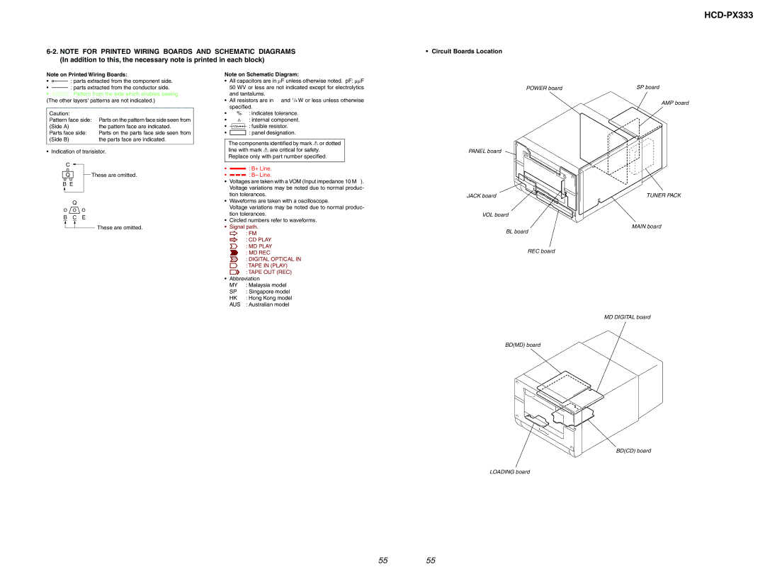
Circuit Boards Location
Side B
Schematic Diagram BD CD Board
Location
Printed Wiring Board BD MD Board
Semiconductor
5959
IC B/D
Printed Wiring Board MD Digital Section
Schematic Diagram MD Digital /3
See page 79 for IC Block Diagrams
See page 79 for IC Block Diagrams
Semiconductor Location
IC B/D
HCD-PX333
Printed Wiring Board SP Board
Printed Wiring Board AMP Board
Schematic Diagram AMP Board
Schematic Diagram SP Board
IC602
Printed Wiring Board Panel
Schematic Diagram Panel
See page 55 for Circuit Boards Location
7474
Schematic Diagram Power Board
I2SLRCKOUT
Waveforms
BD CD Board BD MD Board
MD Digital Board Main Board
IC101 CXA2523AR BD MD Board
IC Block Diagrams
IC141 BH6519FS-E2 BD MD Board
IC1005 uDA1360TS MD Digital Board
IC931 M62016L Main Board
IC PIN Function Description
BD MD Board IC151 CXD2662R
Asyo
Xcas
XWE
Mvci
Sfdr
Frdr
FS4
Srdr
Darst
Reset
LVL1
LVL0
VCC1
Xelt
WR-PWR
I2CCLK
VSS4
VCC3
VSS3
VCC4
CLK
Reset XT1
Drvdat
Drvclk
CLP POS
IN-SW
LOD POS
LOD NEG
Main Board IC501 ∝PDSS3033AYGF-M18-3BA System Controller
KBD CHK
MD/CD Power
GC Power
TR Relay
Self Write
PC Power
Sircs
RDS CLK
REC Board
Section Exploded Views
58 A-4476-550-A Panel BOARD, Complete
LCD601 1-804-371-11 Indicator TUBE, Liquid Crystal
Chassis
162 153 156 161 163
152 151
163
154
303
311 305 313
314 310 309 319
308
360 356 359
359
357 355 354 352
365 370 353 366353 369
522 501 517 514 518 516 502 519 520 515 521
CD Mechanism Deck Section CDM55A-21BD53
510 505 508 511 504
506 512 513
HCD-PX333 Section AMP Electrical Parts List
Diode F1J6TP
HCD-PX333 BD MD
TANTAL. Chip
Elect Chip
Jack
Jack HCD-PX333 Loading Main
HCD-PX333 Main
AEP,UK
MY,SP,HK,AUS
HCD-PX333 Main MD Digital
CONNECTOR, FFC 31P
MD Digital BOARD, Complete Capacitor
MD Digital Panel
HCD-PX333 Panel Power
HCD-PX333 Power REC
HCD-PX333 VOL
111
HCD-PX333 Revision History