|
|
|
|
|
|
|
|
|
|
|
|
|
|
|
|
|
|
|
|
|
|
|
|
|
|
|
|
|
|
|
| ||||
1 | 2 | 3 | 4 | 5 | 6 | 7 | 8 | 9 | 10 | 11 |
|
| 12 | 13 | 14 |
|
|
A |
| MAIN BOARD | (SIDE A) |
|
|
|
|
|
|
|
|
|
|
|
|
| |
|
|
|
|
|
|
|
|
|
|
|
|
|
|
|
|
| |
B |
|
|
|
|
|
|
|
|
| E | 12 | 10 | 7 |
|
|
|
|
|
|
|
|
|
|
|
|
|
|
|
|
|
| ||||
|
|
|
|
|
|
|
|
| 13 |
|
| 6 |
|
|
|
| |
|
|
|
|
|
|
|
|
|
|
|
|
|
| • Semiconductor | |||
|
|
|
|
|
|
|
|
|
| 15 |
|
| 5 |
|
| ||
|
|
|
|
|
|
| S801 |
|
| IC 301 |
|
| Location | ||||
|
|
|
|
|
|
|
|
|
|
|
| ||||||
|
|
|
|
|
|
|
|
|
|
|
|
|
|
|
| ||
|
|
|
|
|
|
|
|
|
| 18 |
|
| 1 |
|
| Ref. No. | Location |
|
|
|
|
|
|
|
|
|
|
| 19 |
| 24 |
|
| ||
|
|
|
|
|
|
|
|
|
|
|
|
|
|
|
| ||
|
|
|
|
| * |
|
|
|
|
|
|
|
|
|
| D101 | |
C |
|
|
|
|
|
|
|
|
|
|
|
|
|
|
|
| |
|
|
|
| IC 601 |
|
|
|
| C301 |
|
|
|
|
| D201 | ||
|
|
|
|
|
|
|
|
|
|
|
|
|
|
| |||
|
|
|
|
|
|
|
|
|
|
|
|
|
|
| D801 | ||
|
|
|
|
| CSP (Chip Size Package) |
|
|
|
|
|
|
|
|
|
| D855 | |
|
|
|
|
|
|
|
|
| S806 |
|
|
|
|
|
| D902 | |
|
|
|
|
|
|
|
|
| GROUP |
|
|
|
|
|
| D903 | |
|
|
|
|
|
|
|
|
|
|
|
|
|
|
|
| IC301 | |
D |
|
|
|
|
|
|
|
|
|
|
|
|
|
|
| IC501 | |
|
|
|
|
|
|
|
|
|
|
|
|
|
|
|
| IC601 | |
|
|
|
|
|
|
|
|
|
|
|
|
|
|
|
| IC901 | |
|
|
|
|
|
|
|
|
|
|
|
|
|
|
|
| Q301 | |
|
|
|
|
|
|
|
|
|
|
|
|
|
|
|
| Q501 | |
|
|
|
|
|
|
|
|
|
|
|
|
|
|
|
| Q901 | |
E |
|
|
|
|
|
|
|
|
|
|
|
|
|
|
| Q902 | |
|
|
|
|
|
|
|
|
| S803 |
|
|
|
|
|
| Q903 | |
|
|
|
|
| S808 |
|
|
|
|
|
|
|
|
|
|
|
|
|
|
|
|
| HOLD |
|
|
|
|
|
|
|
|
|
|
|
|
|
|
|
|
|
|
| S804 |
|
|
|
|
|
|
|
|
|
|
|
|
|
|
| ON |
| VOL- |
|
|
|
|
|
|
|
|
|
|
F |
|
|
|
|
|
|
|
|
|
|
|
|
|
|
|
| |
|
|
|
|
|
|
|
|
|
|
|
|
|
|
|
|
| |
DRY BATTERY |
|
|
|
| OFF |
|
|
|
|
|
|
|
|
|
|
|
|
SIZE "AA" |
|
|
|
|
|
|
|
|
|
|
|
|
|
|
|
| |
(IEC DESIGNATION LR6) |
|
|
|
|
|
|
|
|
|
|
|
|
|
|
|
|
|
1PC, 1.5V |
|
|
|
|
|
|
|
|
|
|
|
|
|
|
|
|
|
G |
|
|
|
|
|
|
|
| (INFO) |
|
|
|
| IC 901 |
|
|
|
|
|
|
|
|
|
|
|
|
|
|
|
|
|
|
|
| |
|
|
|
|
|
| S805 |
|
| S802 |
|
|
|
|
|
|
|
|
|
|
|
|
|
| VOL+ |
|
|
|
|
|
|
|
|
|
|
|
H |
|
| E |
| IC 501 |
|
|
|
|
|
|
|
|
|
|
|
|
|
|
|
|
|
|
|
|
|
|
|
|
|
| 12 |
| ||
|
|
|
|
|
|
|
|
|
|
|
|
|
|
|
| (12) |
|
I |
|
|
|
|
|
|
|
|
|
|
|
|
|
|
|
|
|
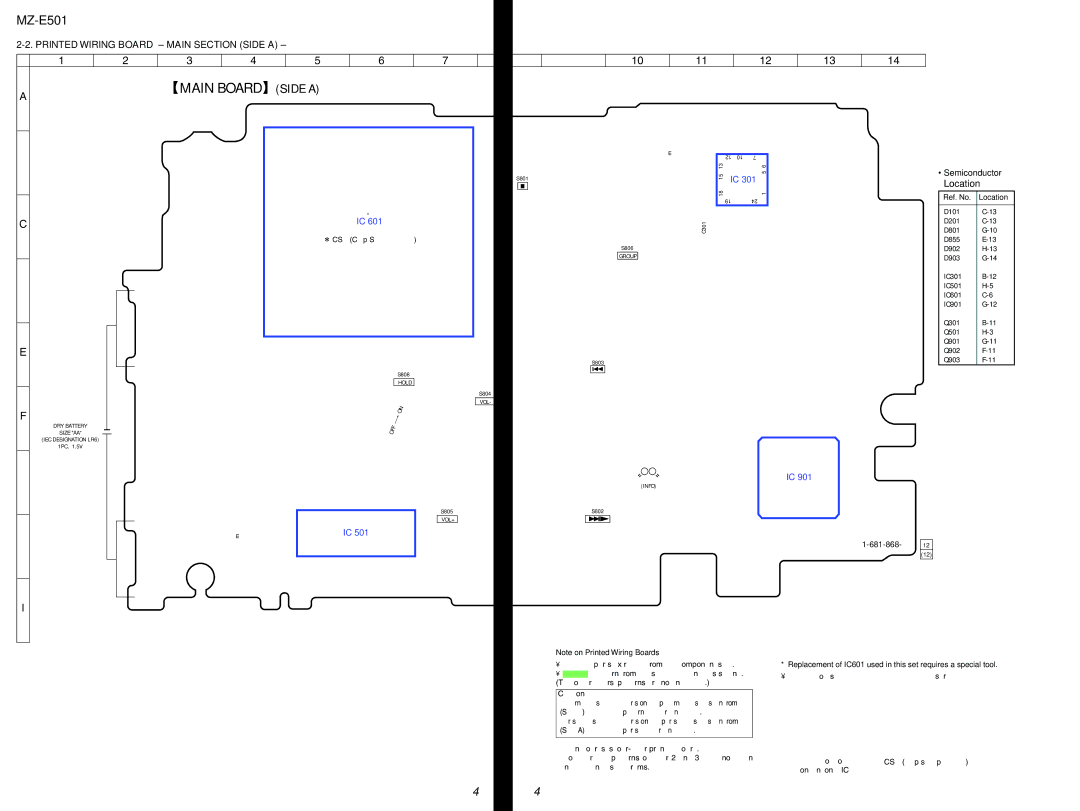
Note on Printed Wiring Boards
•X : parts extracted from the component side.
•![]() : Pattern from the side which enables seeing. (The other layers' patterns are not indicated.)
: Pattern from the side which enables seeing. (The other layers' patterns are not indicated.)
Caution: |
|
Pattern face side: | Parts on the pattern face side seen from the |
(Side B) | pattern face are indicated. |
Parts face side: | Parts on the parts face side seen from the |
(Side A) | parts face are indicated. |
|
|
•Main boards is
However, the patterns of layer 2 and 3 have not been included in this diagrams.
*Replacement of IC601 used in this set requires a special tool.
• Lead Layouts | surface |
Lead layout of | CSP (chip size package) |
conventional IC |
|
44