MZ-E501
SECTION 6
DIAGRAMS
Note on Printed Wiring Boards: MAIN SECTION
•X : parts extracted from the component side.
•![]() : Pattern from the side which enables seeing. (The other layers' patterns are not indicated.)
: Pattern from the side which enables seeing. (The other layers' patterns are not indicated.)
Caution: |
|
Pattern face side: | Parts on the pattern face side seen from the |
(Side B) | pattern face are indicated. |
Parts face side: | Parts on the parts face side seen from the |
(Side A) | parts face are indicated. |
|
|
•Main boards is
However, the patterns of layer 2 and 3 have not been included in this diagrams.
*Replacement of IC601 used in this set requires a special tool.
•Lead Layouts
surface
Lead layout of | CSP (chip size package) |
conventional IC |
|
Note on Schematic Diagram: MAIN SECTION
•All capacitors are in ∝F unless otherwise noted. pF: ∝∝F 50 WV or less are not indicated except for electrolytics and tantalums.
•All resistors are in Ω and 1/4 W or less unless otherwise specified.
•f : internal component.
Note: The components identified by mark 0or dotted line with mark 0are critical for safety.
Replace only with part number specified.
•![]() : B+ Line.
: B+ Line.
•Power voltage is dc 1.5V and fed with regulated dc power supply from battery terminal.
•Voltages and waveforms are dc with respect to ground under
no mark : PLAY
•Voltages are taken with a VOM (Input impedance 10 MΩ). Voltage variations may be noted due to normal produc- tion tolerances.
•Waveforms are taken with a oscilloscope.
Voltage variations may be noted due to normal produc- tion tolerances.
•Circled numbers refer to waveforms.
•Signal path.
F : Audio (Analog)
J : Audio (Digital)
*Replacement of IC601 used in this set requires a special tool.
•The voltage and waveform of CSP (chip size package) cannot be measured, because its lead layout is different from that of conventional IC.
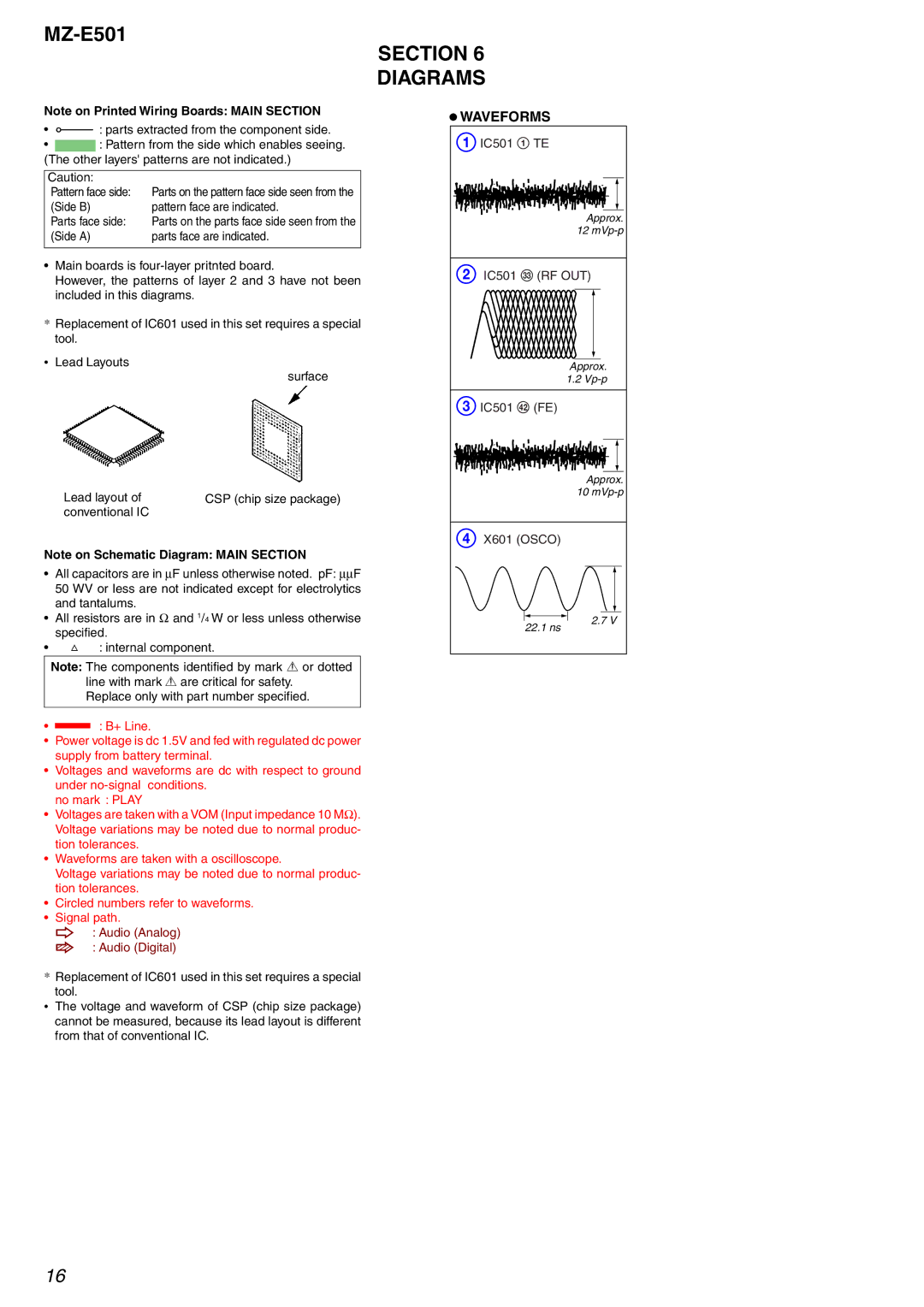
rWAVEFORMS
1 IC501 1 TE |
Approx. |
12 |
2 IC501 ed (RF OUT) |
Approx. |
1.2 |
3 IC501 rs (FE) |
Approx. |
10 |
4 X601 (OSCO) |
2.7 V |
22.1 ns |
16