MZ-E501
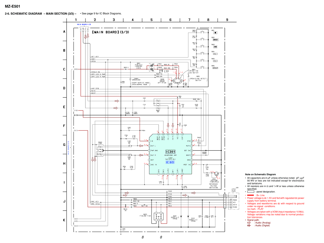
2-6. SCHEMATIC DIAGRAM – MAIN SECTION (3/3) – • See page 9 for IC Block Diagrams.
 IC B/D
Note on Schematic Diagram
• All capacitors are in ∝ F unless otherwise noted. pF: ∝∝ F 50 WV or less are not indicated except for electrolytics and tantalums.
• All resistors are in Ω and 1/4 W or less unless otherwise specified.
• C : panel designation.
• |
| : B+ Line. |
| ||
| ||
• | Power voltage is dc 1.5V and fed with regulated dc power | |
| supply from battery terminal. | |
• | Voltages and waveforms are dc with respect to ground | |
| under | |
| no mark : PLAY | |
• | Voltages are taken with a VOM (Input impedance 10 MΩ ). | |
| Voltage variations may be noted due to normal produc- | |
| tion tolerances. | |
• | Signal path. | |
| F : Audio (Analog) | |
| J : Audio (Digital) | |
88