MZ-E501
Pin No. | Pin Name | I/O | Description | |
|
|
|
| |
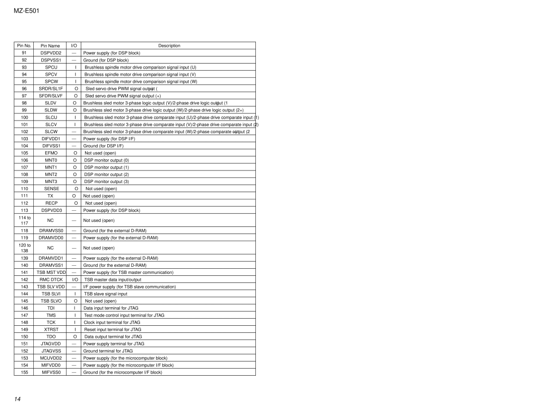
91 | DSPVDD2 | — | Power supply (for DSP block) | |
92 | DSPVSS1 | — | Ground (for DSP block) | |
|
|
|
| |
93 | SPCU | I | Brushless spindle motor drive comparison signal input (U) | |
94 | SPCV | I | Brushless spindle motor drive comparison signal input (V) | |
|
|
|
| |
95 | SPCW | I | Brushless spindle motor drive comparison signal input (W) | |
96 | SRDR/SL1F | O | Sled servo drive PWM signal output | |
|
|
|
| |
97 | SFDR/SLVF | O | Sled servo drive PWM signal output (+) | |
|
|
|
| |
98 | SLDV | O | Brushless sled motor | |
|
|
|
| |
99 | SLDW | O | Brushless sled motor | |
|
|
|
| |
100 | SLCU | I | Brushless sled motor | |
|
|
|
| |
101 | SLCV | I | Brushless sled motor | |
102 | SLCW | — | Brushless sled motor | |
|
|
|
| |
103 | DIFVDD1 | — | Power supply (for DSP I/F) | |
|
|
|
| |
104 | DIFVSS1 | — | Ground (for DSP I/F) | |
105 | EFMO | O | Not used (open) | |
|
|
|
| |
106 | MNT0 | O | DSP monitor output (0) | |
107 | MNT1 | O | DSP monitor output (1) | |
|
|
|
| |
108 | MNT2 | O | DSP monitor output (2) | |
109 | MNT3 | O | DSP monitor output (3) | |
|
|
|
| |
110 | SENSE | O | Not used (open) | |
|
|
|
| |
111 | TX | O | Not used (open) | |
|
|
|
| |
112 | RECP | O | Not used (open) | |
113 | DSPVDD3 | — | Power supply (for DSP block) | |
|
|
|
| |
114 to | NC | — | Not used (open) | |
117 | ||||
|
|
| ||
|
|
|
| |
118 | DRAMVSS0 | — | Ground (for the external | |
|
|
|
| |
119 | DRAMVDD0 | — | Power supply (for the external | |
120 to | NC | — | Not used (open) | |
138 | ||||
|
|
| ||
|
|
|
| |
139 | DRAMVDD1 | — | Power supply (for the external | |
140 | DRAMVSS1 | — | Ground (for the external | |
|
|
|
| |
141 | TSB MST VDD | — | Power supply (for TSB master communication) | |
142 | RMC DTCK | I/O | TSB master data input/output | |
|
|
|
| |
143 | TSB SLV VDD | — | I/F power supply (for TSB slave communication) | |
|
|
|
| |
144 | TSB SLVI | I | TSB slave signal input | |
145 | TSB SLVO | O | Not used (open) | |
|
|
|
| |
146 | TDI | I | Data input terminal for JTAG | |
147 | TMS | I | Test mode control input terminal for JTAG | |
|
|
|
| |
148 | TCK | I | Clock input terminal for JTAG | |
149 | XTRST | I | Reset input terminal for JTAG | |
|
|
|
| |
150 | TDO | O | Data output terminal for JTAG | |
|
|
|
| |
151 | JTAGVDD | — | Power supply terminal for JTAG | |
152 | JTAGVSS | — | Ground terminal for JTAG | |
|
|
|
| |
153 | MCUVDD2 | — | Power supply (for the microcomputer block) | |
154 | MIFVDD0 | — | Power supply (for the microcomputer I/F block) | |
|
|
|
| |
155 | MIFVSS0 | — | Ground (for the microcomputer I/F block) |
14