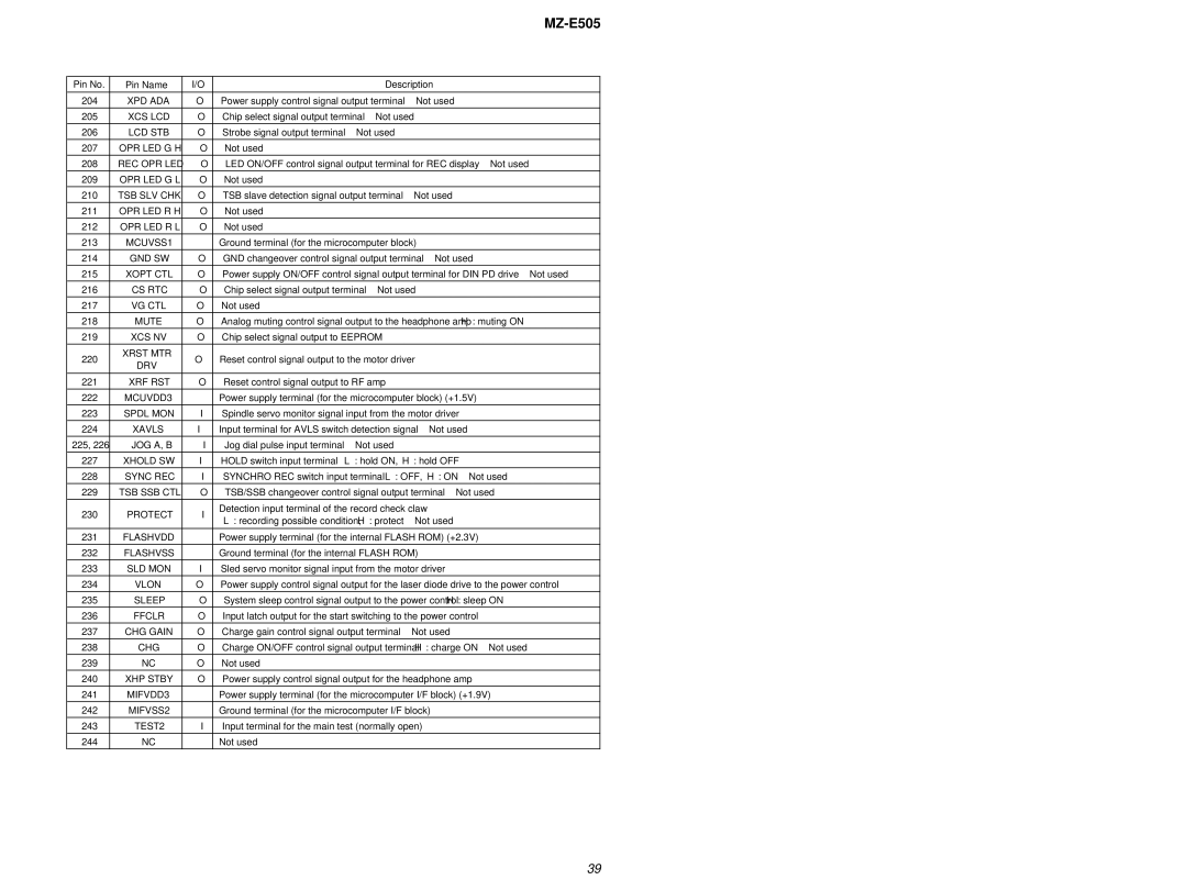
MZ-E505 specifications
The Sony MZ-E505 is a portable mini-disc player that emerged in the early 2000s as part of Sony's innovative move towards digital audio solutions. This compact device combines functionality, versatility, and cutting-edge technology, making it a popular choice among music enthusiasts. The MZ-E505 stands out due to its sleek design and impressive features, setting the standard for portable audio players of its time.One of the main characteristics of the MZ-E505 is its lightweight design, weighing approximately 160 grams. Its portability is complemented by an elegant, user-friendly interface, which includes a simple set of buttons for easy navigation through tracks and folders. The device features a bright LCD display that shows essential information such as track number, time elapsed, and battery life, ensuring users remain informed while on the go.
The MZ-E505's standout feature is its mini-disc technology, allowing users to record and playback high-quality audio. Mini-discs, introduced by Sony in the 1990s, offer an advanced storage solution that can hold up to 74 minutes of high-fidelity stereo sound on the standard format. The player also supports LP2 and LP4 modes, enabling users to double or quadruple the recording capacity, which is perfect for those who require more space for their music collections.
In terms of sound quality, the MZ-E505 utilizes Sony’s ATRAC (Adaptive Transform Acoustic Coding) compression technology, which ensures that audio playback is clear and precise. The device is equipped with a 20-second shock protection mechanism to prevent interruptions during playback, giving users peace of mind while enjoying their favorite tracks during activities like jogging or commuting.
Battery life is another crucial aspect, and the MZ-E505 doesn’t disappoint. It features a rechargeable battery that can provide up to 10 hours of continuous playback on a full charge. Additionally, users have the option to utilize standard AA batteries as an alternative power source.
The MZ-E505 also incorporates a variety of connectivity options, including an analog line-in for direct recording from external sources. This feature was particularly appealing for audiophiles who wanted to create their mix compilations.
Overall, the Sony MZ-E505 is a remarkable blend of portability, sound quality, and innovative technology, representing the quintessential qualities of early digital audio devices. Although the mini-disc format has since been largely superseded by other digital technologies, the MZ-E505 remains a cherished piece of audio history, celebrated for its unique capabilities and breathtaking design.
