SECTION 4
DIAGRAMS
THIS NOTE IS COMMON FOR PRINTED WIRING BOARDS AND SCHEMATIC DIAGRAMS. (In addition to this, the necessary note is printed in each block.)
|
|
SCHEMATIC DIAGRAM |
For Printed Wiring Boards.
Note:
•Y: Parts extracted from the conductor side.
•![]() : Pattern from the side which enables seeing. (The other layers' patterns are not indicated.)
: Pattern from the side which enables seeing. (The other layers' patterns are not indicated.)
Caution: |
|
Pattern face side: | Parts on the pattern face side seen |
(SIDE B) | from the pattern face are indicated. |
Parts face side: | Parts on the parts face side seen from |
(SIDE A) | the parts face are indicated. |
•MAIN board is
However, the patterns of
•Lead layouts
surface
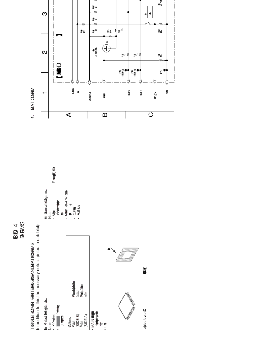
For Schematic Diagrams.
Note:
•All capacitors are in μF unless otherwise noted. (p: pF) 50 WV or less are not indicated except for electrolytics and tantalums.
•All resistors are in Ω and 1/4 W or less unless otherwise specified.
•C: Panel designation.
•A: B+ Line.
| 1 | 2 |
| 3 |
|
| 4 |
|
| 5 | 6 |
| MAIN BOARD |
|
|
|
|
|
|
| CN881 |
| |
A |
|
|
|
|
|
|
|
|
|
| |
|
|
|
|
|
|
|
|
| 11P |
| |
EXTRST |
|
|
|
|
|
|
|
| 1 | GND | |
|
|
|
|
|
|
|
|
| |||
| NC_ON |
|
|
|
|
|
|
|
| 2 | NC |
|
|
| R893 |
|
|
|
|
|
| 3 | FR |
|
|
| 470k |
|
|
|
|
|
| ||
|
|
|
|
|
|
|
|
|
|
| |
| VDD_GP1_J |
|
|
|
|
|
|
|
| 4 | PLAY |
|
|
|
|
|
|
|
|
| 5 | FF | |
|
| Q881 | R897 | R886 | R887 | R895 |
|
|
| ||
|
| 0 | 47k | 47k | 100 | R896 |
|
| 6 | VOL+ | |
|
|
|
|
|
|
| 100 |
|
| ||
|
|
|
|
|
|
|
|
|
|
| |
B | KEY_WAKE |
|
|
|
|
|
|
|
| 7 | VOL- |
S |
|
|
|
|
|
|
| 8 | RESET | ||
| R883 |
|
|
|
|
|
| ||||
|
|
| 470k |
|
|
|
|
|
| 9 |
|
|
|
|
|
|
|
|
|
|
|
| |
|
|
| R882 |
|
|
|
|
|
| 10 |
|
| CL881 | R884 |
|
| R888 | R889 |
| C883 | 11 | GND | |
| (KEY_AD0) | 1k |
|
|
| ||||||
|
| 1k |
|
|
| 10k | 10k |
| 0.01 |
|
|
| KEY_AD0 |
|
|
|
|
|
|
|
|
|
|
| CL882 | R885 |
|
|
|
| R890 | R891 | C884 |
|
|
| (KEY_AD1) |
|
|
|
| 0.01 |
|
| |||
|
| 1k |
|
|
|
| 10k | 10k |
|
|
|
| KEY_AD1 |
|
|
|
|
|
|
|
|
|
|
Lead layout of conventional IC | CSP (Chip Size Package) |
C |
|
| S881 |
|
|
|
|
| HOLD |
| CL884 | CL886 | |
|
|
|
| |||
XHOLD_KEY |
|
|
|
|
|
|
CL883 | R881 | R892 | C881 | C882 |
|
|
470k | 470k | 0.047 | 0.047 | CL885 | CL887 | |
DGND |
|
|
|
| (GND) |
|
|
|
|
|
|
|
Note 1: In this set, only a part of parts that relate to the switch are supplied. Therefore, the schematic diagram excerpts and has described only a part. Replace a part according to “METHOD OF JUDGING RIGHT AND WRONG OF PARTS RELATED TO SWITCH” (page 7) in servicing notes. Exchange the entire mounted board when parts that do not correspond to it are defective.
Note 2: When the MAIN board is replaced, there are some notes. Refer to “NOTE THE MAIN BOARD REPLACING” (page 4) in servicing notes for notes.
27 27