Chapter 1: Introduction
CH A0,A1 B0,B1 C0,C1 D0,D1 |
| VRM |
| |||
|
|
| ||||
|
|
|
| |||
|
|
|
| |||
|
|
| ||||
8x DIMM |
|
|
|
| ||
|
|
|
| |||
|
|
|
|
|
|
|
|
|
|
|
|
|
|
HT Link
| VRM | CH | A0,A1 B0,B1 C0,C1 D0,D1 | ||
|
| ||||
|
|
|
|
| |
|
|
| |||
|
|
| 8x DIMM | ||
|
|
| |||
|
|
|
|
|
|
|
|
|
|
|
|
|
|
|
|
|
|
| HT |
|
|
|
| VRM |
|
| Link |
8x DIMM | |||||||
|
|
| |||||
|
|
| |||||
|
|
| |||||
|
|
|
|
|
|
|
|
|
|
|
|
|
|
|
|
HT Link
Intel
82576
HT |
|
Link | VRM |
|
|
| HT Link | ||
PCIE (x4) |
|
|
| ||
|
|
| |||
AMD | |||||
|
| ||||
|
| ||||
|
| SR5690 | |||
|
|
|
|
| |
8x DIMM
| PCIE (X4) |
| LSI |
| PCIE (X16) |
| SAS2 2008 |
|
|
| |
|
| SLOT#4 | |
|
|
| PCIE_(X16) |
VGA ![]()
Winbond
WPCM450
SATA
![]()
![]()
![]() AMD
AMD ![]() USB
USB ![]() SP5100
SP5100 ![]()
![]()
6x PORTS SATA_CONN
USB PORT
LPC BUS
H/W_MONITOR
W83795
9_FAN_CONN.
LPC SIO
Keyboard/
Mouse
FWH
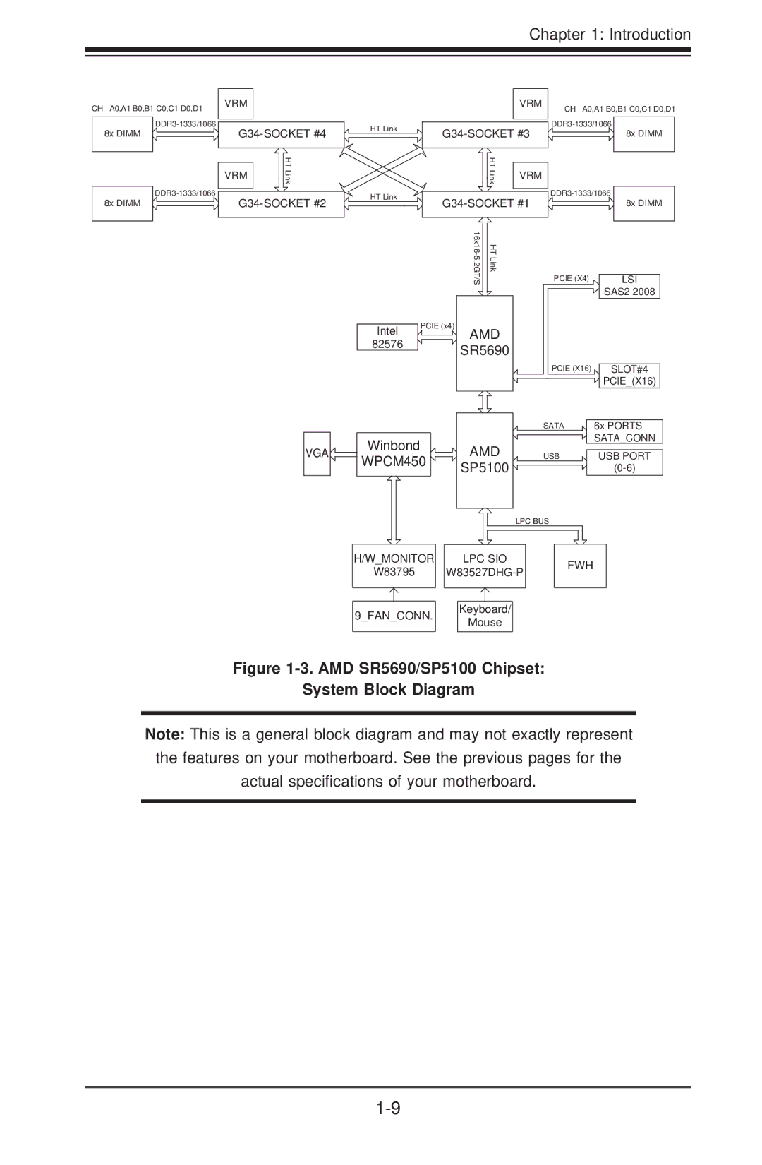
Figure 1-3. AMD SR5690/SP5100 Chipset:
System Block Diagram
Note: This is a general block diagram and may not exactly represent the features on your motherboard. See the previous pages for the actual specifications of your motherboard.