Tyan S1857
Motherboard User’s Manual Revision
Table of Contents
107
Overview
Chapter
Icons
Voltage and Power
Physical Dimensions
Processor Information
Please refer to page 26 for current PII CPU
Software Specifications
Bios Information
Disk Drive & System I/O
Creative Labs ES 1373 PCI
S1857 & S1857A VIA Chipset Hardware Specifications/Features
Audio S1857A only
Win98 SE, Windows NT 4.0 & SP
Returning Merchandise for Service
Technical Support
Help resources
For Resellers Only
This page left blank intentionally
Installation
How to install our products right...the first time
Unpacking
What’s the first thing I should do?
Installation Steps
Do Notapplypowertothe Board Ifithas Been Damaged
Pin jumpers
Quick References for Jumpers
Off on
Map of Motherboard Jumpers
Map of S1857 Features
Setting Jumpers
CPU Speed Settings Jumpers JP10, JP11, JP12, JP13
Panel Connector Settings Jumper J16
Power LED
Fan Speed Detect
Cmos RTC
Mounting the Motherboard in the Chassis
Installing Memory
This Operates on 3.3 volt standby for theDIMM banks
Chapter
Pin Dimm
Cache Memory
Dimm Bank Total
Installing the CPU and Cooling Fan
Installing CPU Retention Modules
Install
Secure module here
Connecting IDE and Floppy Drives
Pin
Connecting Floppy Drives
Connecting the Power Supply
Installing Add-on Cards
Power up when the card is inserted into the slot
Connecting PS/2, USB, Serial & Parallel Devices
Connecting Com and Printer Ports
You are done
3chapter Bios Configuration
Main Setup
Key Function
System Date/Time
Floppy Drive a and B
Type How to Configure
Entering Drive Parameters
Parameter Description
Default Settings
Boot Sector Virus Protection
Optimal Defaults
Fail-Safe Defaults
Advanced Cmos Setup
Advanced Cmos Setup Default Settings Chart
Settings Chart
Advanced Setup
Quick Boot
1st Boot Device
2nd Boot Device
3rd Boot Device
Try Other Boot Devices
Boot Up Num-Lock
Password Check
Boot To OS/2
System Bios Cacheable
Cache Bus ECC
Default Primary Video
C000,16K Shadow and C400,16K Shadow
Chipset Setup
Advanced Chipset Setup Default Settings Chart
USB Function
PIIX4 SERR#
BX Master Latency Timer Clks
Multi-Trans Timer Clks
USB KB/Mouse Legacy Support
Port 64/60 Emulation
PCI1 to PCI0 Access
Sdram RAS# to CAS# Delay
Power Down Sdram
Method of Memory Detection
AGPMulti-Trans Timer AGP Clks
AGP Low-Priority Timer Clks
AGP Parity Error Response
8bit I/O Recovery Time
USB Passive Release
PIIX4 Passive Release
TypeF DMABuffer Control1
DMA-nType
Power Management Setup
Power Management Setup Default Settings Chart
Power Management/APM
Power Button Function
Green PC Monitor Power State
ACPIAware O/S
Video Power Down Mode
Hard Disk Power Down Mode
Power Saving Type
Standby/Suspend Timer Unit
PC98 Power LED
Slow Clock Ratio
Display Activity
LAN Wake-up
Plug and Play Setup
RTC Wake-up
Plug and Play Setup Default Settings Chart
IRQ15
PCI Latency Timer PCI Clocks
Plug and PlayAware O/S
PCI VGA Palette Snoop
Allocate IRQ to PCI VGA
OffBoard PCI IDE Primary IRQ
Offboard PCI IDE Secondary IRQ
PCI Slot n IRQ Priority
DMA Channel n
Reserved Memory Address
Bios Devnode for Shadow RAM
PCI Device Search Order
Peripheral Setup
Peripheral Setup Default Settings Chart
Power Interruption
Overclock Warning Message
KeyboardWake-up Function
Mouse Wake-up Function
Serial Port2 Mode
IR Transmission Mode
Mode Description
Onboard Serial Port1
Parallel Port Mode
EPPVersion
Parallel Port IRQ
Parallel Port DMA Channel
Set Supervisor Password Enter Set User Password Enter
Supervisor and User Security
Language Utility
Flash Writer Utility
This page left blank intentionally
System Resources
Beep Codes
Troubleshooting System Problems
Beeps Error Message Description
Displayed Error Messages
Error Message Line Press F1 to continue
Error Message Explanation
Error in the second DMA channel
1Appendix Glossary
Appendix
Glossary
Doze mode, only the CPU’s speed is slowed
Glossary
Appendix
Glossary
Appendix
2Appendix Retention Module Installation
LowerTabs
Figure B
Figure D
RemoveCPU
Installing SECC2 CPUs Option
Figure H
Introduction to Setup
Starting Setup
Case of Problems
Setup Keys
Getting Help
Key Function
Main Setup Menu
Setup Variations
Standard Cmos Setup
Bios Features Setup
Chipset Features Setup
Power Management Setup
Standard Cmos Setup
Exit Without Saving
Date
Time
Hard Disks
Video
Drive A, Drive B
Halt On
Bios Features Setup
Memory
Bios Feature Setup Default Settings Chart
Se tting Option Bios De fault Se tup De fault
Quick Power On Self Test
Boot Sequence
Virus Warning
CPU Internal Cache/External Cache
Boot Up Floppy Seek
Boot Up NumLock Status
IDE HDD Block Mode
Typematic Rate Setting
Typematic Delay Msec
Video Bios Shadow
Security Option
PCI/VGA Palette Snoop
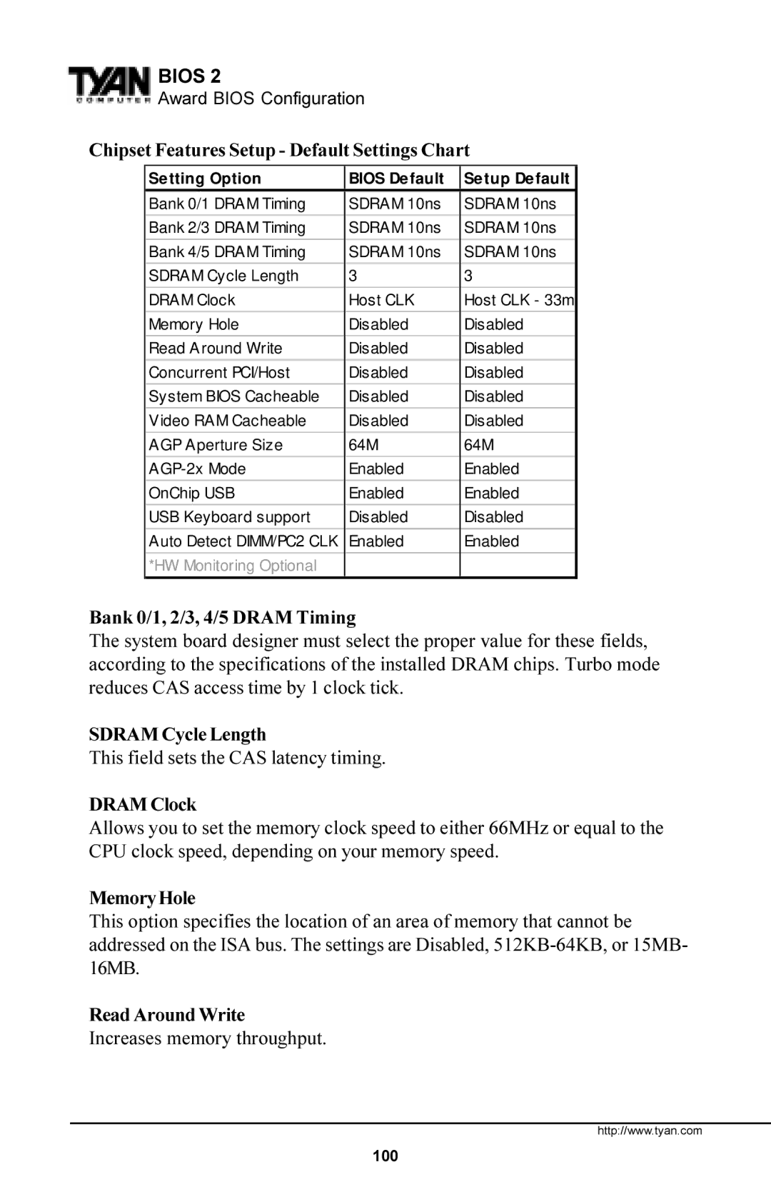
Chipset Features Setup
Advanced Options
Chipset Features Setup Default Settings Chart
Bank 0/1, 2/3, 4/5 Dram Timing
Sdram Cycle Length
Dram Clock
Concurrent PCI/Host
Video RAM Cacheable
AGP Aperture Size AGP-2xMode
OnChip USB
Power Management Setup
Power Management Setup Default Settings Chart
Acpi Function
Power Management
PM Control by APM
PM Timers
HDDPowerDown
Video Off Option
Video Off Method
Suspend Mode
RTC Alarm Resume
DozeMode
PM Events
IRQ3 COM2
PnP/PCI Configuration
PnP / PCI Configuration Default Settings Chart
PNP OS Installed
Reset Configuration Data
Resources Controlled By
IRQ-nAssigned to
PCI Delay Transaction
PCI#2 Access #1 Retry
PCI Dynamic Bursting
PCI Master 0 WS Write
Integrated Peripherals Default Settings Chart
Integrated Peripherals
IDE Prefetch Mode
Power on Function
On-Chip PCI IDE First/Second Channel
IDE Primary/Secondary Master/Slave PIO
Onboard Parallel Mode
KBC Input Clock
Onboard FDC Controller
Onboard Serial Port 1
User Password
Flash Writer Utility
Bios
Flash Memory Writer
Document # D1367-120
Jumper Settings Quick Reference
See pages 15-20 for details on Jumpers