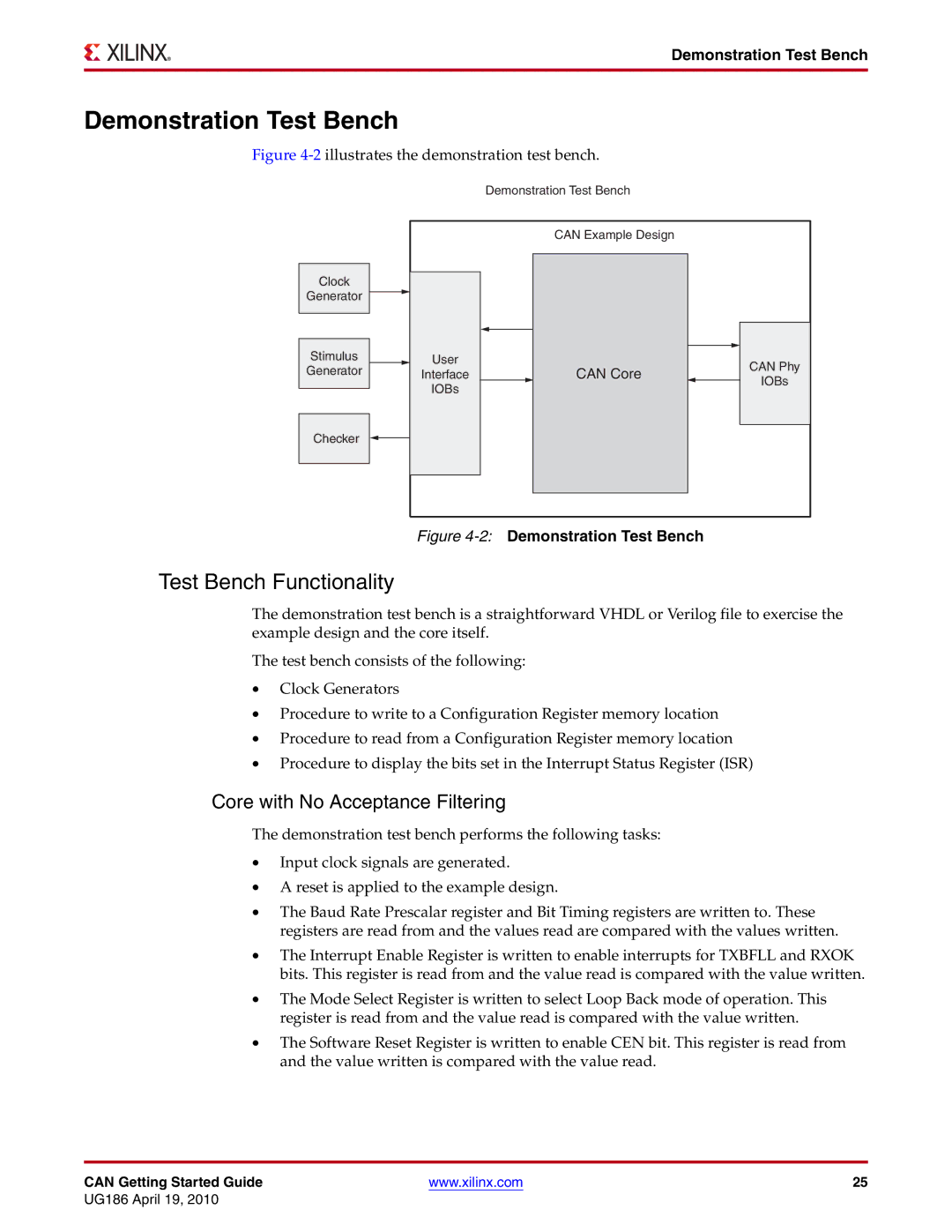
Clock
Generator
Stimulus
Generator
Checker
Demonstration Test Bench
| CAN Example Design |
| |
User | CAN Core | CAN Phy | |
Interface | |||
IOBs | |||
IOBs |
| ||
|
| ||
Figure |
| ||
Test Bench Functionality
The demonstration test bench is a straightforward VHDL or Verilog file to exercise the example design and the core itself.
The test bench consists of the following:
•Clock Generators
•Procedure to write to a Configuration Register memory location
•Procedure to read from a Configuration Register memory location
•Procedure to display the bits set in the Interrupt Status Register (ISR)
Core with No Acceptance Filtering
The demonstration test bench performs the following tasks:
•Input clock signals are generated.
•A reset is applied to the example design.
•The Baud Rate Prescalar register and Bit Timing registers are written to. These registers are read from and the values read are compared with the values written.
•The Interrupt Enable Register is written to enable interrupts for TXBFLL and RXOK bits. This register is read from and the value read is compared with the value written.
•The Mode Select Register is written to select Loop Back mode of operation. This register is read from and the value read is compared with the value written.
•The Software Reset Register is written to enable CEN bit. This register is read from and the value written is compared with the value read.
CAN Getting Started Guide | www.xilinx.com | 25 |
UG186 April 19, 2010