Upstream
System ACE
Interface
Connector
Upstream
Interface
Connector
2x
LVTTL
2x Diff Pair
Clocks
SMA SMA
LEDs
![]() VBATT
VBATT
Virtex-4 DUT
Configuration |
Port |
To Test Points |
on All Pins |
PROGRAM |
User RESET |
Downstream |
|
|
|
System ACE |
|
| Downstream |
Interface |
|
| Interface |
Connector |
|
| Connector |
|
|
|
|
Power Bus and Switches
5V Jack
LVTTL 2x
SMA SMA
2x Diff Pair Clocks
DONE INIT ![]() LED
LED ![]() LED
LED
VCCINT
![]() VCC Jack
VCC Jack
VCCO
![]() VCCO Jack
VCCO Jack
![]() VCCAUX
VCCAUX ![]() VCCAUX Jack
VCCAUX Jack
VCC3
![]() VCC1V8
VCC1V8 ![]()
AVCC
UG078_01_101204
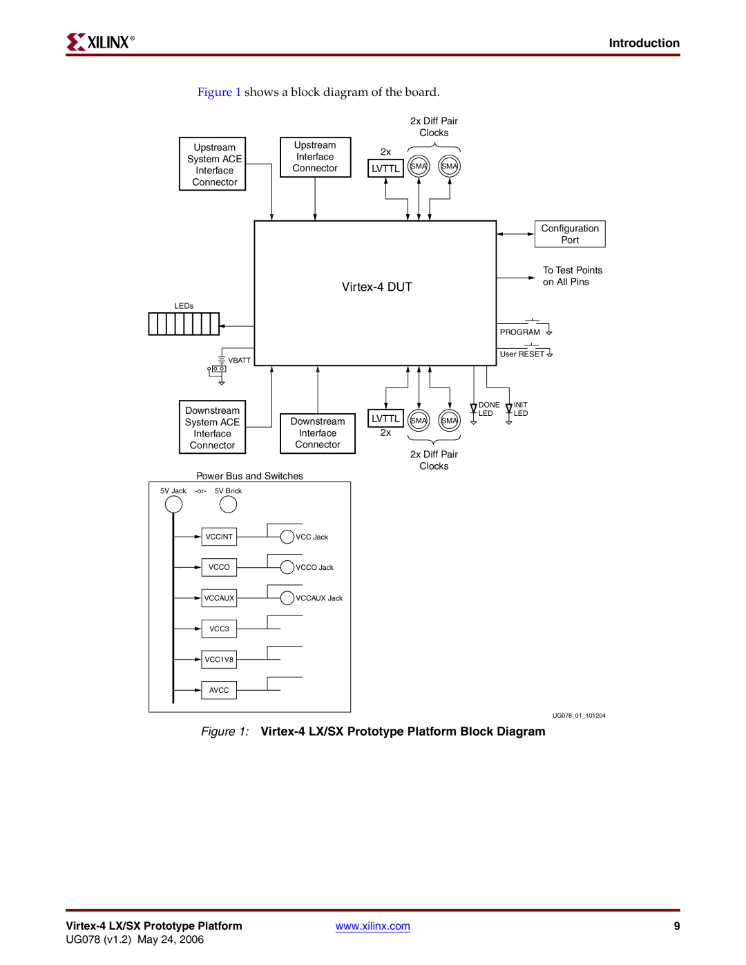
Figure 1: Virtex-4 LX/SX Prototype Platform Block Diagram
| www.xilinx.com | 9 |
UG078 (v1.2) May 24, 2006