Detailed Description
R
11. Differential Clock Inputs
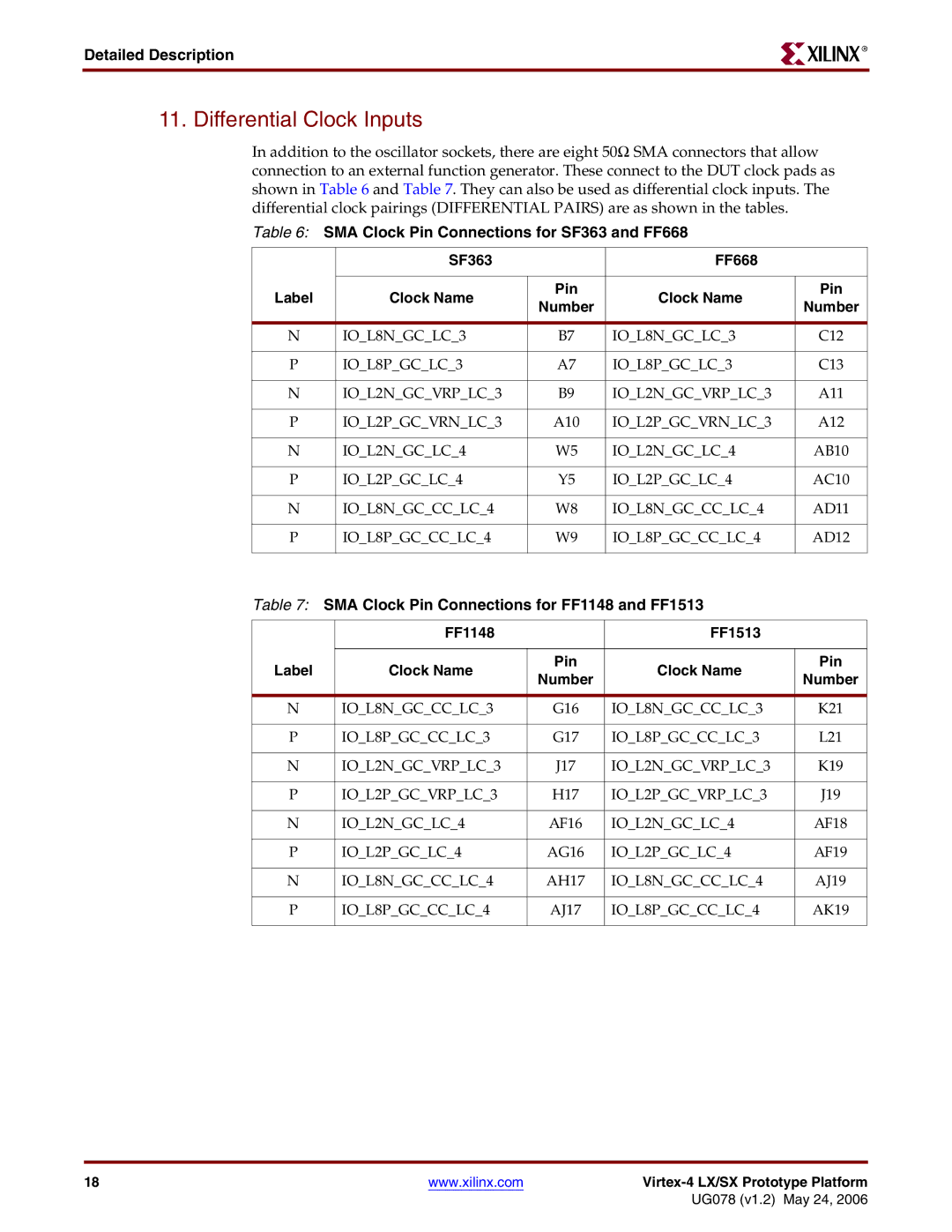
In addition to the oscillator sockets, there are eight 50Ω SMA connectors that allow connection to an external function generator. These connect to the DUT clock pads as shown in Table 6 and Table 7. They can also be used as differential clock inputs. The differential clock pairings (DIFFERENTIAL PAIRS) are as shown in the tables.
Table 6: SMA Clock Pin Connections for SF363 and FF668
| SF363 |
| FF668 |
| |
|
|
|
|
| |
Label | Clock Name | Pin | Clock Name | Pin | |
Number | Number | ||||
|
|
| |||
|
|
|
|
| |
N | IO_L8N_GC_LC_3 | B7 | IO_L8N_GC_LC_3 | C12 | |
|
|
|
|
| |
P | IO_L8P_GC_LC_3 | A7 | IO_L8P_GC_LC_3 | C13 | |
|
|
|
|
| |
N | IO_L2N_GC_VRP_LC_3 | B9 | IO_L2N_GC_VRP_LC_3 | A11 | |
|
|
|
|
| |
P | IO_L2P_GC_VRN_LC_3 | A10 | IO_L2P_GC_VRN_LC_3 | A12 | |
|
|
|
|
| |
N | IO_L2N_GC_LC_4 | W5 | IO_L2N_GC_LC_4 | AB10 | |
|
|
|
|
| |
P | IO_L2P_GC_LC_4 | Y5 | IO_L2P_GC_LC_4 | AC10 | |
|
|
|
|
| |
N | IO_L8N_GC_CC_LC_4 | W8 | IO_L8N_GC_CC_LC_4 | AD11 | |
|
|
|
|
| |
P | IO_L8P_GC_CC_LC_4 | W9 | IO_L8P_GC_CC_LC_4 | AD12 | |
|
|
|
|
|
Table 7: SMA Clock Pin Connections for FF1148 and FF1513
| FF1148 |
| FF1513 |
| |
|
|
|
|
| |
Label | Clock Name | Pin | Clock Name | Pin | |
Number | Number | ||||
|
|
| |||
|
|
|
|
| |
N | IO_L8N_GC_CC_LC_3 | G16 | IO_L8N_GC_CC_LC_3 | K21 | |
|
|
|
|
| |
P | IO_L8P_GC_CC_LC_3 | G17 | IO_L8P_GC_CC_LC_3 | L21 | |
|
|
|
|
| |
N | IO_L2N_GC_VRP_LC_3 | J17 | IO_L2N_GC_VRP_LC_3 | K19 | |
|
|
|
|
| |
P | IO_L2P_GC_VRP_LC_3 | H17 | IO_L2P_GC_VRP_LC_3 | J19 | |
|
|
|
|
| |
N | IO_L2N_GC_LC_4 | AF16 | IO_L2N_GC_LC_4 | AF18 | |
|
|
|
|
| |
P | IO_L2P_GC_LC_4 | AG16 | IO_L2P_GC_LC_4 | AF19 | |
|
|
|
|
| |
N | IO_L8N_GC_CC_LC_4 | AH17 | IO_L8N_GC_CC_LC_4 | AJ19 | |
|
|
|
|
| |
P | IO_L8P_GC_CC_LC_4 | AJ17 | IO_L8P_GC_CC_LC_4 | AK19 | |
|
|
|
|
|
18 | www.xilinx.com |
|
|
| UG078 (v1.2) May 24, 2006 |