R
Detailed Description
12. DUT Socket
The DUT socket contains the user FPGA, referred to as the device under test (DUT). The DUT must be oriented using the P1 indicator on the board.
Caution! Failure to insert the device to the proper orientation can damage the device. To avoid pin damage, always use the vacuum tool provided when inserting or removing the
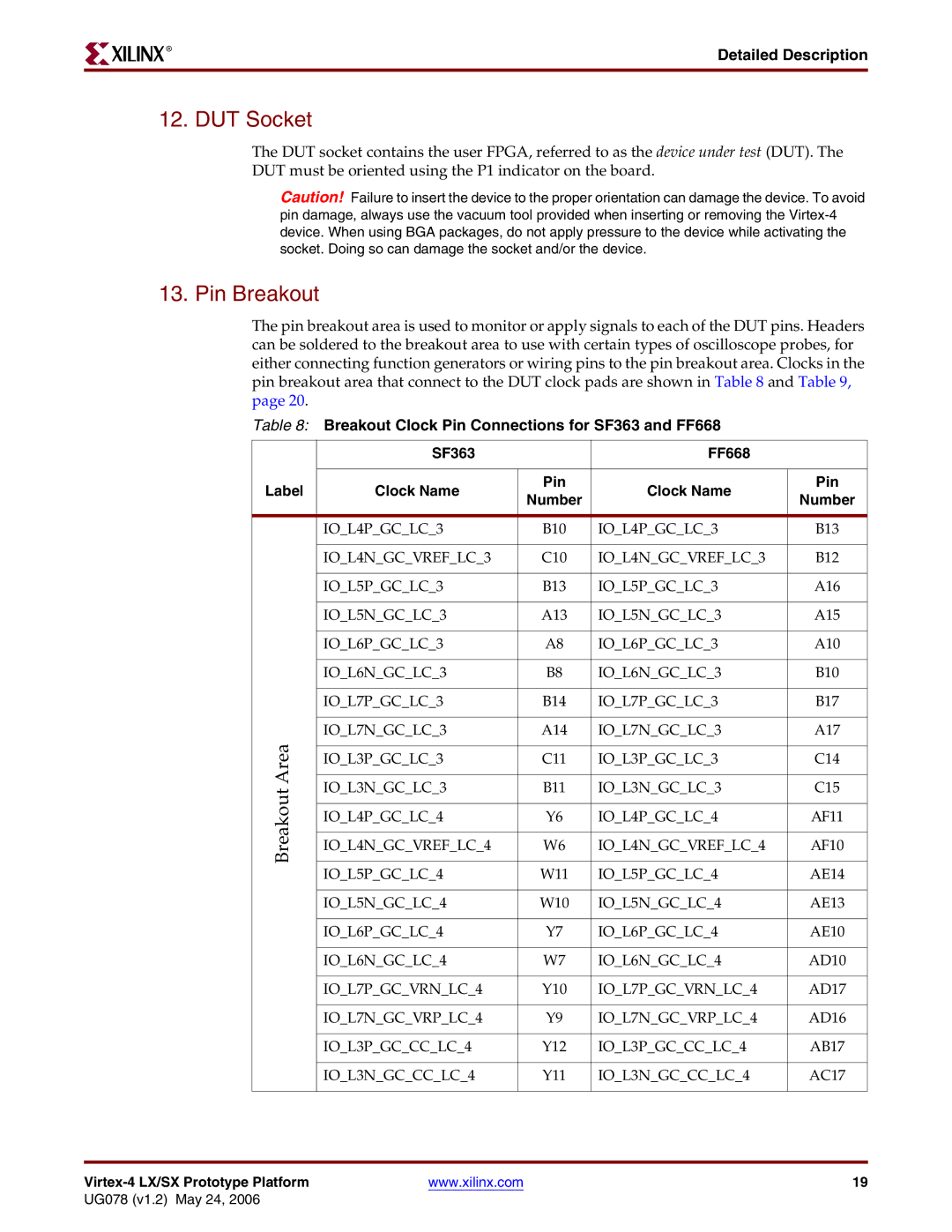
13. Pin Breakout
The pin breakout area is used to monitor or apply signals to each of the DUT pins. Headers can be soldered to the breakout area to use with certain types of oscilloscope probes, for either connecting function generators or wiring pins to the pin breakout area. Clocks in the pin breakout area that connect to the DUT clock pads are shown in Table 8 and Table 9, page 20.
Table 8: Breakout Clock Pin Connections for SF363 and FF668
| SF363 |
| FF668 |
| |
|
|
|
|
| |
Label | Clock Name | Pin | Clock Name | Pin | |
Number | Number | ||||
|
|
| |||
|
|
|
|
| |
| IO_L4P_GC_LC_3 | B10 | IO_L4P_GC_LC_3 | B13 | |
|
|
|
|
| |
| IO_L4N_GC_VREF_LC_3 | C10 | IO_L4N_GC_VREF_LC_3 | B12 | |
|
|
|
|
| |
| IO_L5P_GC_LC_3 | B13 | IO_L5P_GC_LC_3 | A16 | |
|
|
|
|
| |
| IO_L5N_GC_LC_3 | A13 | IO_L5N_GC_LC_3 | A15 | |
|
|
|
|
| |
| IO_L6P_GC_LC_3 | A8 | IO_L6P_GC_LC_3 | A10 | |
|
|
|
|
| |
| IO_L6N_GC_LC_3 | B8 | IO_L6N_GC_LC_3 | B10 | |
|
|
|
|
| |
| IO_L7P_GC_LC_3 | B14 | IO_L7P_GC_LC_3 | B17 | |
|
|
|
|
| |
Area | IO_L7N_GC_LC_3 | A14 | IO_L7N_GC_LC_3 | A17 | |
|
|
|
| ||
IO_L3P_GC_LC_3 | C11 | IO_L3P_GC_LC_3 | C14 | ||
| |||||
|
|
|
|
| |
Breakout | IO_L3N_GC_LC_3 | B11 | IO_L3N_GC_LC_3 | C15 | |
|
|
|
| ||
IO_L4P_GC_LC_4 | Y6 | IO_L4P_GC_LC_4 | AF11 | ||
| |||||
|
|
|
|
| |
| IO_L4N_GC_VREF_LC_4 | W6 | IO_L4N_GC_VREF_LC_4 | AF10 | |
|
|
|
|
| |
| IO_L5P_GC_LC_4 | W11 | IO_L5P_GC_LC_4 | AE14 | |
|
|
|
|
| |
| IO_L5N_GC_LC_4 | W10 | IO_L5N_GC_LC_4 | AE13 | |
|
|
|
|
| |
| IO_L6P_GC_LC_4 | Y7 | IO_L6P_GC_LC_4 | AE10 | |
|
|
|
|
| |
| IO_L6N_GC_LC_4 | W7 | IO_L6N_GC_LC_4 | AD10 | |
|
|
|
|
| |
| IO_L7P_GC_VRN_LC_4 | Y10 | IO_L7P_GC_VRN_LC_4 | AD17 | |
|
|
|
|
| |
| IO_L7N_GC_VRP_LC_4 | Y9 | IO_L7N_GC_VRP_LC_4 | AD16 | |
|
|
|
|
| |
| IO_L3P_GC_CC_LC_4 | Y12 | IO_L3P_GC_CC_LC_4 | AB17 | |
|
|
|
|
| |
| IO_L3N_GC_CC_LC_4 | Y11 | IO_L3N_GC_CC_LC_4 | AC17 | |
|
|
|
|
|
| www.xilinx.com | 19 |
UG078 (v1.2) May 24, 2006