


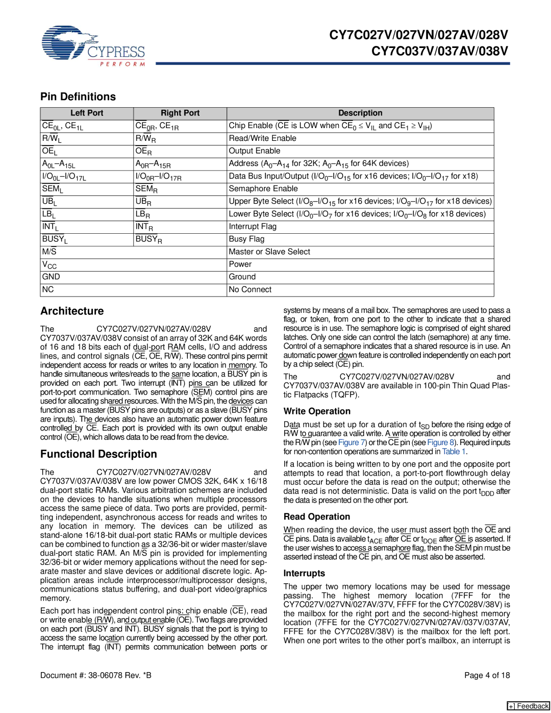


CY7C027V/027VN/027AV/028V
CY7C037V/037AV/038V
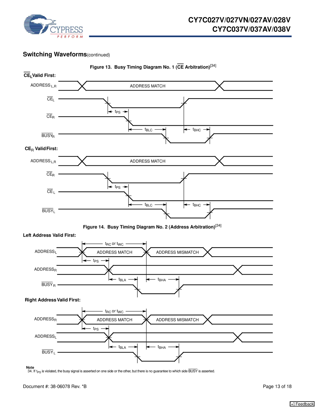
Pin Configurations (continued)
Figure 2. 100-Pin TQFP (Top View)
A9L
A10L
A11L
A12L
A13L
A14L
[2]A15L
LBL
UBL
CE0L
CE1L
SEML
R/WL
OEL
VCC
GND
I/O17L
I/O16L
GND
I/O15L
I/O14L ![]()
I/O13L
I/O12L ![]() I/O11L I/O10L
I/O11L I/O10L
A8L | A7L | A6L | A5L | A4L | A3L | A2L | A1L | A0L |
|
| BUSYL | GND | GND | VCC |
|
| BUSYR |
| INTR | A0R | A1R | A2R | A3R | A4R | A5R | A6R | A7R |
|
|
|
| ||||||||||||||||||||||||
| INTL |
|
|
| |||||||||||||||||||||||
|
| M/S |
| ||||||||||||||||||||||||
|
|
| |||||||||||||||||||||||||
100 99 | 98 | 97 | 96 | 95 | 94 | 93 | 92 | 91 | 90 | 89 | 88 | 87 | 86 | 85 | 84 | 83 | 82 | 81 | 80 | 79 | 78 | 77 | 76 | |
1 |
|
|
|
|
|
|
|
|
|
|
|
|
|
|
|
|
|
|
|
|
|
|
| 75 |
2 |
|
|
|
|
|
|
|
|
|
|
|
|
|
|
|
|
|
|
|
|
|
|
| 74 |
3 |
|
|
|
|
|
|
|
|
|
|
|
|
|
|
|
|
|
|
|
|
|
|
| 73 |
4 |
|
|
|
|
|
|
|
|
|
|
|
|
|
|
|
|
|
|
|
|
|
|
| 72 |
5 |
|
|
|
|
|
|
|
|
|
|
|
|
|
|
|
|
|
|
|
|
|
|
| 71 |
6 |
|
|
|
|
|
|
|
|
|
|
|
|
|
|
|
|
|
|
|
|
|
|
| 70 |
7 |
|
|
|
|
|
|
|
|
|
|
|
|
|
|
|
|
|
|
|
|
|
|
| 69 |
8 |
|
|
|
|
|
|
|
|
|
|
|
|
|
|
|
|
|
|
|
|
|
|
| 68 |
9 |
|
|
|
|
|
|
|
|
|
|
|
|
|
|
|
|
|
|
|
|
|
|
| 67 |
10 |
|
|
|
|
|
|
|
|
|
|
|
|
|
|
|
|
|
|
|
|
|
|
| 66 |
11 |
|
|
|
|
| CY7C038V (64K x 18) |
|
|
|
|
| 65 | ||||||||||||
12 |
|
|
|
|
|
|
|
|
|
| 64 | |||||||||||||
13 |
|
|
|
|
|
|
|
|
|
| 63 | |||||||||||||
|
|
| CY7C037V/037AV (32K x 18) |
|
|
| ||||||||||||||||||
14 |
|
|
|
|
|
| 62 | |||||||||||||||||
15 |
|
|
|
|
|
| 61 | |||||||||||||||||
|
|
|
|
|
|
|
|
|
|
|
|
|
|
|
|
|
|
|
|
|
|
| ||
16 |
|
|
|
|
|
|
|
|
|
|
|
|
|
|
|
|
|
|
|
|
|
|
| 60 |
17 |
|
|
|
|
|
|
|
|
|
|
|
|
|
|
|
|
|
|
|
|
|
|
| 59 |
18 |
|
|
|
|
|
|
|
|
|
|
|
|
|
|
|
|
|
|
|
|
|
|
| 58 |
19 |
|
|
|
|
|
|
|
|
|
|
|
|
|
|
|
|
|
|
|
|
|
|
| 57 |
20 |
|
|
|
|
|
|
|
|
|
|
|
|
|
|
|
|
|
|
|
|
|
|
| 56 |
21 |
|
|
|
|
|
|
|
|
|
|
|
|
|
|
|
|
|
|
|
|
|
|
| 55 |
22 |
|
|
|
|
|
|
|
|
|
|
|
|
|
|
|
|
|
|
|
|
|
|
| 54 |
23 |
|
|
|
|
|
|
|
|
|
|
|
|
|
|
|
|
|
|
|
|
|
|
| 53 |
24 |
|
|
|
|
|
|
|
|
|
|
|
|
|
|
|
|
|
|
|
|
|
|
| 52 |
25 |
|
|
|
|
|
|
|
|
|
|
|
|
|
|
|
|
|
|
|
|
|
|
| 51 |
26 | 27 | 28 | 29 | 30 | 31 | 32 | 33 | 34 | 35 | 36 | 37 | 38 | 39 | 40 | 41 | 42 | 43 | 44 | 45 | 46 | 47 | 48 | 49 | 50 |
A8R
A9R
A10R
A11R
A12R
A13R
A14R A15R [2]
LBR
UBR
CE0R
CE1R
SEMR
R/WR
GND
OER
GND
I/O17R
GND
I/O16R
I/O15R
I/O14R
I/O13R
I/O12R
I/O11R
I/O9L | I/O8L | VCC | I/O7L | I/O6L | I/O5L | I/O4L | I/O3L | I/O2L | GND | I/O1L | I/O0L | GND | I/O0R | I/01R | I/O2R | I/O3R | I/O4R | I/O5R | I/O6R | VCC | I/O7R | I/O8R | I/O9R | I/O10R |
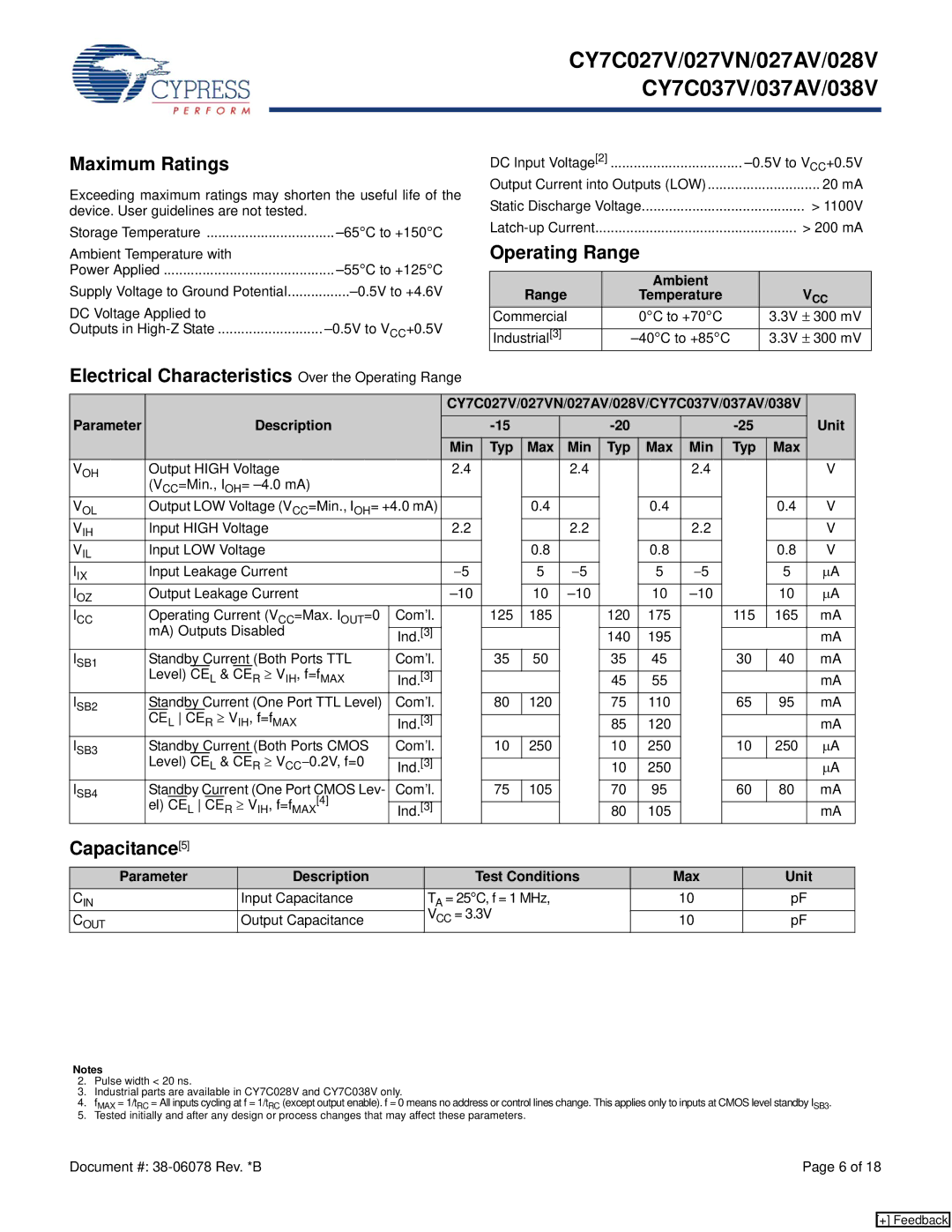
Selection Guide
Parameter | Unit | |||
Maximum Access Time | 15 | 20 | 25 | ns |
|
|
|
|
|
Typical Operating Current | 125 | 120 | 115 | mA |
|
|
|
|
|
Typical Standby Current for ISB1 (Both ports TTL level) | 35 | 35 | 30 | mA |
Typical Standby Current for ISB3 (Both ports CMOS level) | 10 μA | 10 μA | 10 μA | μA |
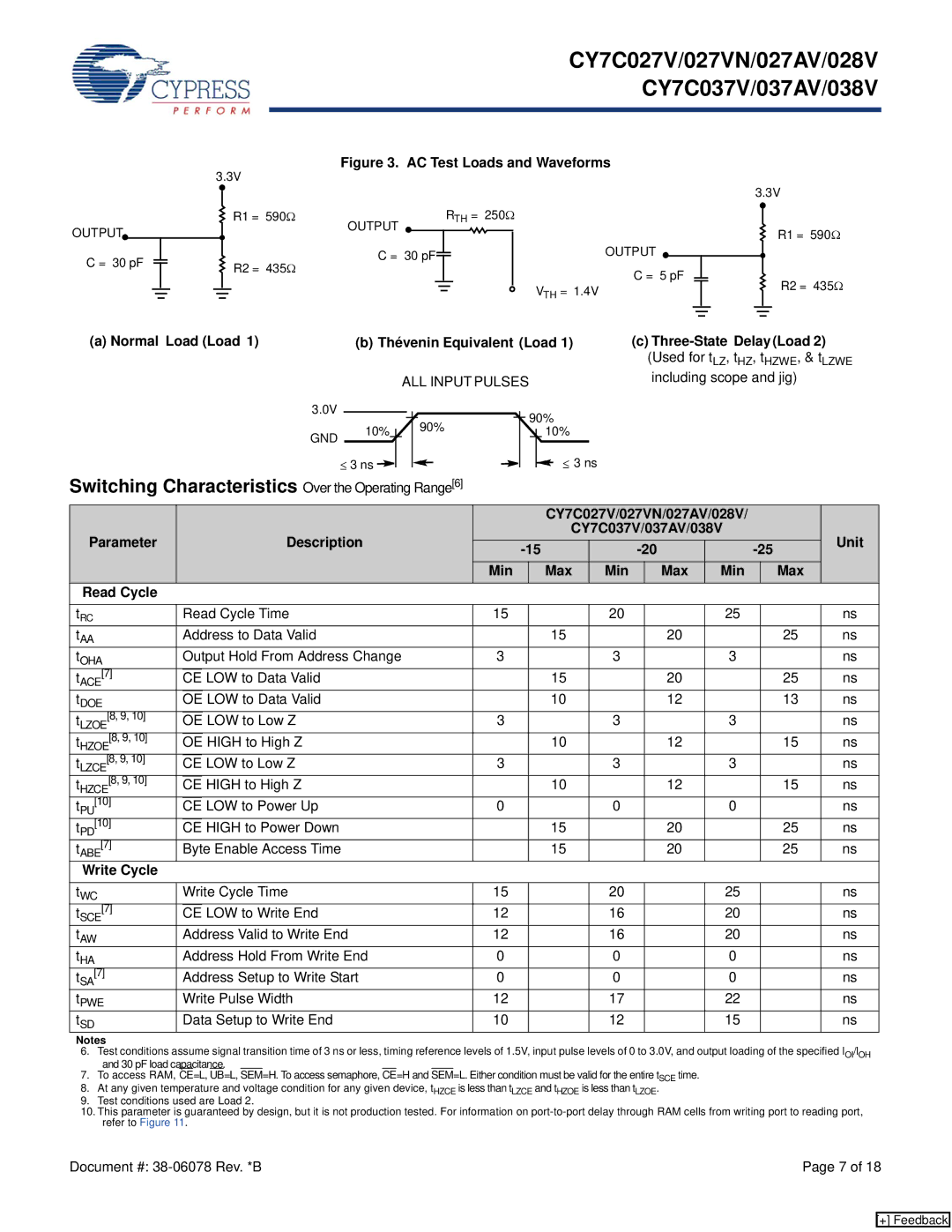
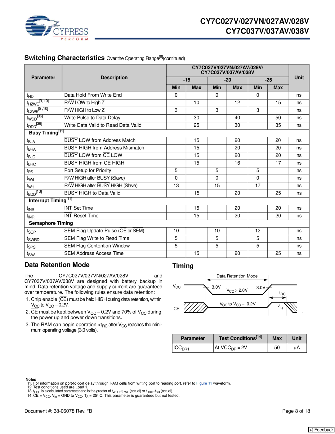
Note
2. This pin is NC for CY7C037V/037AV.
Document #: | Page 3 of 18 |
[+] Feedback