


CY7C027V/027VN/027AV/028V
CY7C037V/037AV/038V
generated to the owner. The interrupt is reset when the owner reads the contents of the mailbox. The message is user defined.
Each port can read the other port’s mailbox without resetting the interrupt. The active state of the busy signal (to a port) prevents the port from setting the interrupt to the winning port. Also, an active busy to a port prevents that port from reading its own mailbox and, thus, resetting the interrupt to it.
If an application does not require message passing, do not connect the interrupt pin to the processor’s interrupt request input pin.
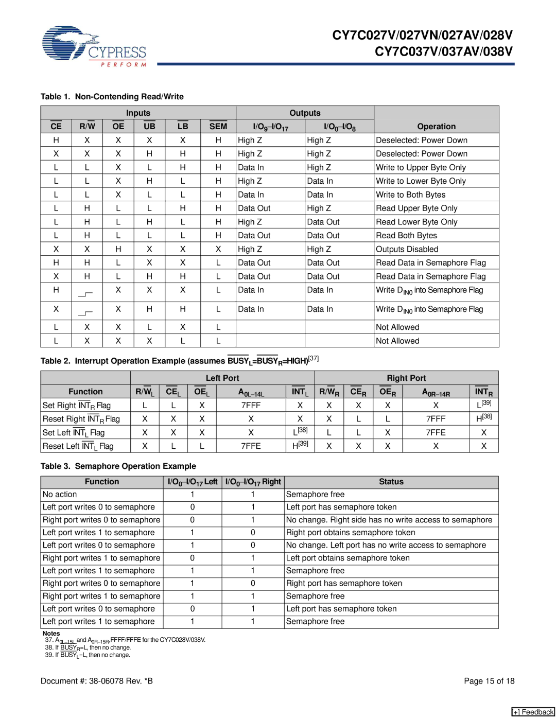
The operation of the interrupts and their interaction with Busy are summarized in Table 2.
Busy
The CY7C027V/027VN/027AV/028V and CY7037V/037AV/038V provide
Master/Slave
AM/S pin is provided to expand the word width by configuring the device as either a master or a slave. The BUSY output of the master is connected to the BUSY input of the slave. This allows the device to interface to a master device with no external components. Writing to slave devices must be delayed until after the BUSY input has settled (tBLC or tBLA), otherwise, the slave chip may begin a write cycle during a contention situation. When tied HIGH, the M/S pin allows the device to be used as a master and, therefore, the BUSY line is an output. BUSY can then be used to send the arbitration outcome to a slave.
Semaphore Operation
The CY7C027V/027VN/027AV/028V and CY7037V/037AV/038V provide eight semaphore latches, which are separate from the
are used to reserve resources that are shared between the two ports.The state of the semaphore indicates that a resource is in use. For example, if the left port wants to request a given resource, it sets a latch by writing a zero to a semaphore location. The left port then verifies its success in setting the latch by reading it. After writing to the semaphore, SEM or OE must be deasserted for tSOP before attempting to read the semaphore. The semaphore value is available tSWRD + tDOE after the rising edge of the semaphore write. If the left port was successful (reads a zero), it assumes control of the shared resource, otherwise (reads a one) it assumes the right port has control and continues to poll the semaphore. When the right side has relinquished control of the semaphore (by writing a one), the left side succeeds in gaining control of the semaphore. If the left side no longer requires the semaphore, a one is written to cancel its request.
Semaphores are accessed by asserting SEM LOW. The SEM pin functions as a chip select for the semaphore latches (CE must remain HIGH during SEM LOW).
When writing to the semaphore, only I/O0 is used. If a zero is written to the left port of an available semaphore, a one appears at the same semaphore address on the right port. That semaphore can now only be modified by the side showing zero (the left port in this case). If the left port now relinquishes control by writing a one to the semaphore, the semaphore is set to one for both sides. However, if the right port had requested the semaphore (written a zero) while the left port had control, the right port would immediately own the semaphore as soon as the left port released it. Table 3 shows sample semaphore operations.
When reading a semaphore, all sixteen/eighteen data lines output the semaphore value. The read value is latched in an output register to prevent the semaphore from changing state during a write from the other port. If both ports attempt to access the semaphore within tSPS of each other, the semaphore is definitely obtained by one side or the other, but there is no guarantee which side controls the semaphore.
Document #: | Page 5 of 18 |
[+] Feedback