Sony DX4, 486DX, AR-B1474 Programming RS-485, Initialize COM port, Send out one character Transmit

Page 66

AR-B1474 User¡¦s Guide

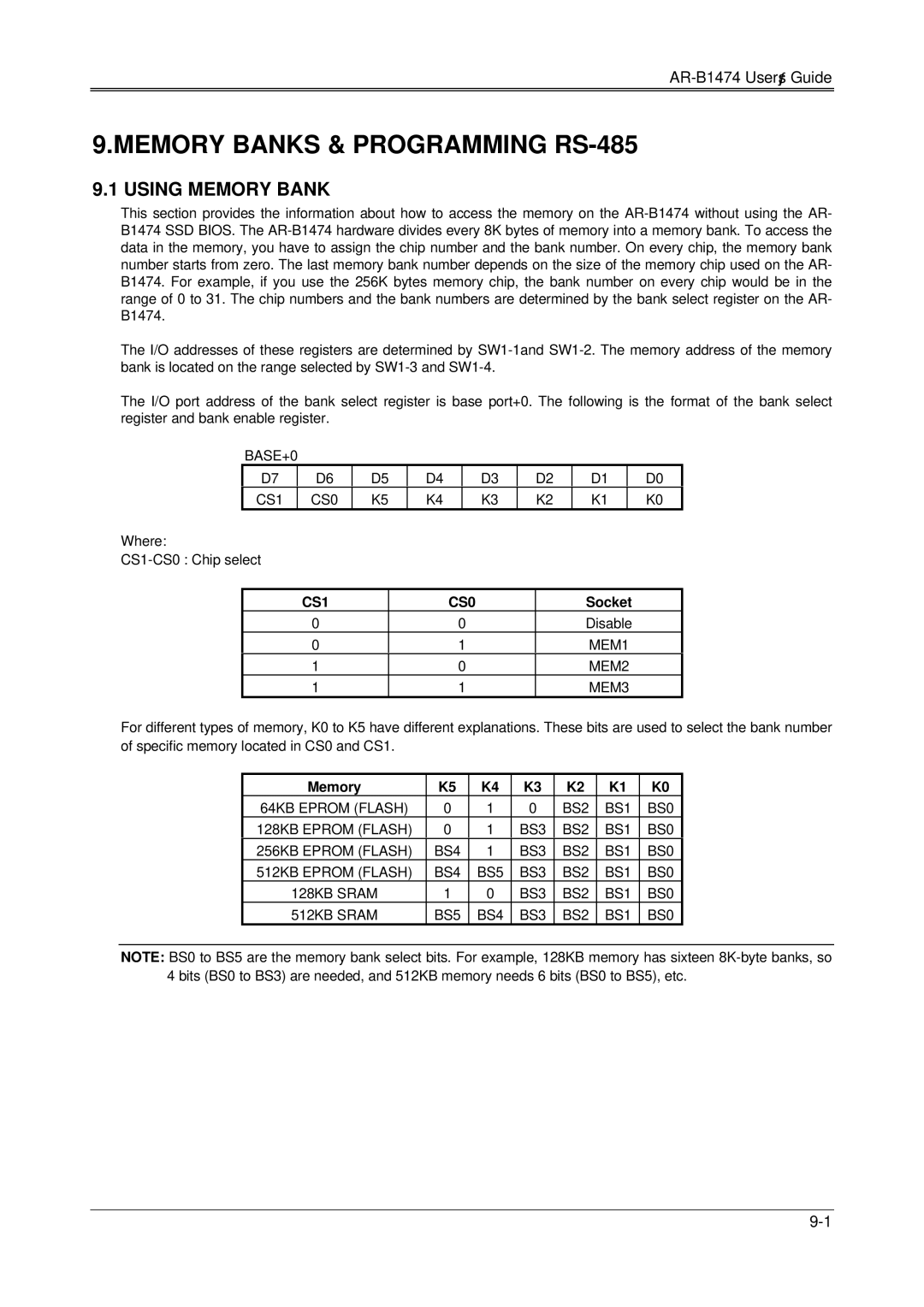
Example 1: Select the 10th bank of the MEM1 on the AR-B1474. The AR-B1474 is using 27C020 (256K*8), and the base port is &H210.

100 base_port=&H210

110 OUT base_port+0,&H59

Example 2: Select the 40th bank of MEM3 on the AR-B1474. The AR-B1474 is using 27C040 (512K*8), and the base port is &H390.

200 base_port=&H390

210 OUT base_port+0,&HD7

9.2 PROGRAMMING RS-485

The majority communicative operation of the RS-485 is in the same of the RS-232. When the RS-485 proceeds the transmission which needs control the TXC signal, and the installing steps are as follows:

Step 1: Enable TXC

Step 2: Send out data

Step 3: Waiting for data empty

Step 4: Disable TXC

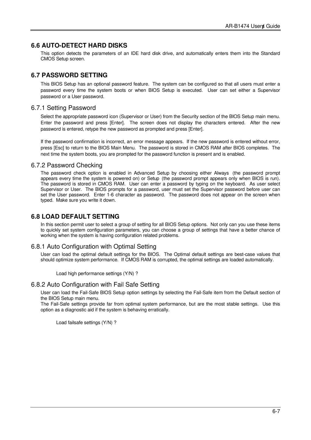
NOTE: Please refer to the section of the “Serial Port” in the chapter “System Control” for the detail description of the COM port’ s register.

(1) Initialize COM port

Step 1: Initialize COM port in the receiver interrupt mode, and /or transmitter interrupt mode. (All of the communication protocol buses of the RS-485 are in the same.)

Step 2: Disable TXC (transmitter control), the bit 0 of the address of offset+4 just sets “0” .

NOTE: Control the AR-B1474 CPU card’ s DTR signal to the RS-485’ s TXC communication.

(2) Send out one character (Transmit)

Step 1: Enable TXC signal, and the bit 0 of the address of offset+4 just sets “1” .

Step 2: Send out the data. (Write this character to the offset+0 of the current COM port address)

Step 3: Wait for the buffer’ s data empty. Check transmitter holding register (THRE, bit 5 of the address of offset+5), and transmitter shift register (TSRE, bit 6 of the address of offset+5) are all sets must be “0” .

Step 4: Disabled TXC signal, and the bit 0 of the address of offset+4 sets “0”

9-2

Image 66
Contents Industrial Grade 486DX/DX2/DX4 CPU Card Page Table of Contents Memory Banks & Programming RS-485 Bios ConsoleSpecifications Placement & Dimensions SSD Types Supported & IndexPreface Static Electricity Precautions OrganizationOverview IntroductionFeatures Packing ListKeyboard Controller System ControllerDMA Controller DMA ControllerInterrupt Controller Interrupt Controller1 I/O Port Address Map Hex Range DeviceI/O Port Address Map Address Description TimerReal-Time Clock and Non-Volatile RAM Real-Time Clock & Non-Volatile RAMISA Bus Pin Assignment ISA Bus Pin AssignmentISA Bus Signal Description Name DescriptionTransmitter Holding Register THR Serial PortReceiver Buffer Register RBR DlabLine Control Register LCR Interrupt Enable Register IERInterrupt Identification Register IIR Modem Control Register MCRDivisor Latch LS, MS Parallel PortModem Status Register MSR Register AddressData Swapper Printer Status BufferPrinter Control Latch & Printer Control Swapper Setting UP the System OverviewSerial Port System SettingRS-232 Connector DB1 & DB2 RS-485 Adapter Select JP3 & JP11Hard Disk IDE Connector CN1 Power Connector J5HDD Pin Assignment FDD Port Connector CN2 Parallel Port Connector CN3CN3 6 PC/104 Connector Pin PC/104 Connector Bus a & B CN6Pin PC/104 Connector Bus C & D CN4 PC/104 ISA Bus Signal Description IRQ 3-7, 9-12, 14CPU Voltage Select JP2 CPU SettingAMD DX2-80 CPU Select JP1 AMD 4X CPU 5x86 Select JP15CPU Clock Setting CPU Clock Select JP6 & JP9Cache RAM Size Select JP8 Memory SettingDram Configuration SIMM1Keyboard Connector LED Header J1, J2 & J4External Speaker Header J3 Reset Header J7Battery Setting CRT Display Type Select JP13Page Installation Utility Diskette PGM1474.EXEWD1474.EXE WP1474.EXEBU1474.EXE Display Error in PGF File Help to PGF FileWrite Protect Function Enable the Software Write ProtectDisable the Software Write Protect Hardware Write ProtectTime-Out Setting Watchdog TimerWatchdog Timer Setting Time Factor Time-Out Period SecondsWatchdog Timer Enabled Watchdog Timer TriggerWatchdog Timer Disabled Page Switch Setting Solid State DiskSSD Firmware Address Select SW1-3 & SW1-4 Overview2 I/O Port Address Select SW1-1 & SW1-2 DEVICE=C\DOS\EMM386.EXE X=C800-CFFFSSD Drive Number SW1-5 & SW1-6 Simulate 2 Disk DriveFlash Eprom Sram ROM Type Select SW1-7 & SW1-8 Disk Drive Name ArrangementJumper Setting SSD Bios Select JP7Switch and Jumper Setting SSD Memory Type Setting M1 ~ M3 & JP5ROM Disk Installation UV Eprom 27CxxxUV Eprom 27CXXX Switch Setting Software Programming5V Large Flash 29FXXX Switch Setting Large Page 5V Flash Disk5V Flash 29CXXX & 28EEXXX Switch Setting Small Page 5V Flash ROM DiskUsing Tool Program Typing DOS CommandJumper Setting RAM DiskSSD Bios Setting JP7 Installation D.O.CHardware Setting Combination of ROM and RAM DiskSoftware Setting O.C. Setting SW1-8Page Bios Console Bios Setup OverviewFloppy Setup Standard Cmos SetupDate & Time Setup Hard Disk SetupAdvanced Cmos Setup Internal Cache Memory IDE Block Mode TransferIDE LBA Mode ShadowAdvanced Chipset Setup Power Management Auto Configuration with Optimal Setting Setting PasswordPassword Checking Auto Configuration with Fail Safe SettingBios Exit Save Settings and ExitExit Without Saving CPU SpecificationsBios PCBPage Placement & Dimensions PlacementDimensions CS1 CS0 Using Memory BankMemory Banks & Programming RS-485 SocketProgramming RS-485 Initialize COM portSend out one character Transmit Receive data Send out one character to COM1Page SSD Types Supported & Index SSD Types Supported10-2 Index Name Function

DX4, AR-B1474, 486DX specifications

The Sony 486DX, AR-B1474, and DX4 are notable examples of advanced computing technologies from the early to mid-1990s, a time when personal computers were rapidly evolving to meet increasing user demands. These systems played a pivotal role in shaping the landscape of modern computing.

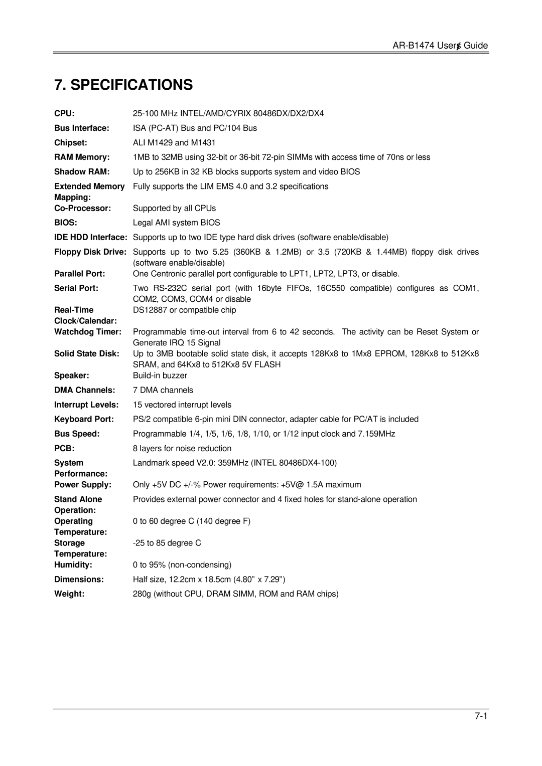
The Sony 486DX is built around the popular Intel 80486 microprocessor, which was a significant step up from its predecessor, the 386. The 486DX featured a 32-bit architecture and introduced integrated cache memory, which greatly enhanced data processing speeds and overall system performance. Operating at clock speeds typically ranging from 25 to 100 MHz, the 486DX models provided a solid foundation for running more sophisticated software applications and advanced games of the era.

Accompanying the 486DX was the AR-B1474 motherboard, designed to maximize the potential of the 486 architecture. This motherboard featured support for up to 512 KB of level 2 cache memory, further boosting performance for data-heavy tasks. The AR-B1474 also included extensive connectivity options, with ISA slots for legacy devices, as well as support for EISA, making it compatible with a wide range of hardware peripherals. This versatility made the AR-B1474 a popular choice among builders of custom desktop PCs during its time.

The DX4, another significant milestone, built upon the 486 architecture by introducing a clock-doubling technique. By effectively allowing the processor to perform operations at up to three times its base clock speed (typically 75 or 100 MHz), the DX4 could handle even more demanding applications, thereby providing users with significant performance improvements without requiring a complete overhaul of their systems.

Both the 486DX and DX4 processors facilitated advancements in multimedia capabilities, with improved graphics rendering and audio performance that supported CD-ROMs and early gaming technologies. This made them particularly appealing to consumers looking for a versatile machine for both work and entertainment.

Overall, the combination of the Sony 486DX, AR-B1474 motherboard, and DX4 processor exemplifies a significant chapter in computing history, showcasing how hardware advancements seamlessly integrated with user needs for performance and flexibility. As these technologies laid the groundwork for future innovations, they remain noteworthy for their contributions to the evolution of personal computing.