Your ePlatform Partner
User’s Manual for Advantech
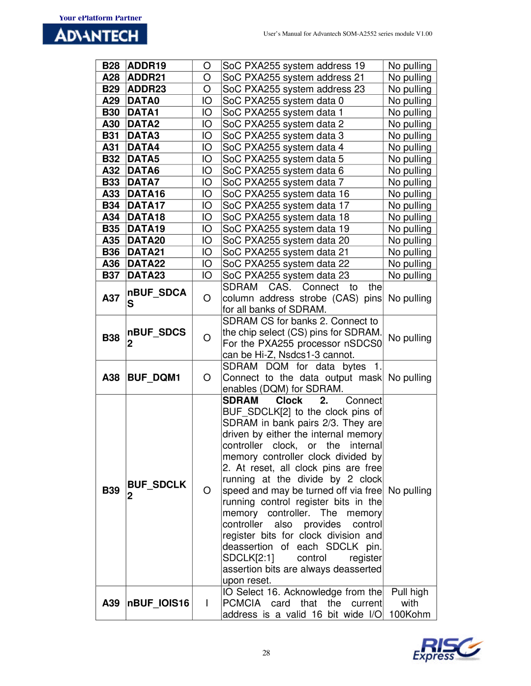
B28 | ADDR19 | O | SoC PXA255 system address 19 |
| No pulling | ||||||
A28 | ADDR21 | O | SoC PXA255 system address 21 |
| No pulling | ||||||
B29 | ADDR23 | O | SoC PXA255 system address 23 |
| No pulling | ||||||
A29 | DATA0 | IO | SoC PXA255 system data 0 |
| No pulling | ||||||
B30 | DATA1 | IO | SoC PXA255 system data 1 |
| No pulling | ||||||
A30 | DATA2 | IO | SoC PXA255 system data 2 |
| No pulling | ||||||
B31 | DATA3 | IO | SoC PXA255 system data 3 |
| No pulling | ||||||
A31 | DATA4 | IO | SoC PXA255 system data 4 |
| No pulling | ||||||
B32 | DATA5 | IO | SoC PXA255 system data 5 |
| No pulling | ||||||
A32 | DATA6 | IO | SoC PXA255 system data 6 |
| No pulling | ||||||
B33 | DATA7 | IO | SoC PXA255 system data 7 |
| No pulling | ||||||
A33 | DATA16 | IO | SoC PXA255 system data 16 |
| No pulling | ||||||
B34 | DATA17 | IO | SoC PXA255 system data 17 |
| No pulling | ||||||
A34 | DATA18 | IO | SoC PXA255 system data 18 |
| No pulling | ||||||
B35 | DATA19 | IO | SoC PXA255 system data 19 |
| No pulling | ||||||
A35 | DATA20 | IO | SoC PXA255 system data 20 |
| No pulling | ||||||
B36 | DATA21 | IO | SoC PXA255 system data 21 |
| No pulling | ||||||
A36 | DATA22 | IO | SoC PXA255 system data 22 |
| No pulling | ||||||
B37 | DATA23 | IO | SoC PXA255 system data 23 |
| No pulling | ||||||
| nBUF_SDCA |
| SDRAM | CAS. | Connect | to | the |
| |||
A37 | O | column address strobe (CAS) pins | No pulling | ||||||||
S | |||||||||||
|
|
| for all banks of SDRAM. |
|
|
| |||||
|
|
| SDRAM CS for banks 2. Connect to |
| |||||||
B38 | nBUF_SDCS | O | the chip select (CS) pins for SDRAM. | No pulling | |||||||
| 2 |
| For the PXA255 processor nSDCS0 |
| |||||||
|
|
| can be |
|
| ||||||
|
|
| SDRAM DQM for data bytes 1. |
| |||||||
A38 | BUF_DQM1 | O | Connect to the data output mask | No pulling | |||||||
|
|
| enables (DQM) for SDRAM. |
|
|
| |||||
|
|
| SDRAM |
| Clock | 2. | Connect |
| |||
|
|
| BUF_SDCLK[2] to the clock pins of |
| |||||||
|
|
| SDRAM in bank pairs 2/3. They are |
| |||||||
|
|
| driven by either the internal memory |
| |||||||
|
|
| controller clock, or the internal |
| |||||||
|
|
| memory controller clock divided by |
| |||||||
|
|
| 2. At reset, all clock pins are free |
| |||||||
| BUF_SDCLK |
| running | at | the | divide by | 2 clock |
| |||
B39 | O | speed and may be turned off via free | No pulling | ||||||||
2 | |||||||||||
|
|
| running control register bits in the |
| |||||||
|
|
| memory | controller. | The | memory |
| ||||
|
|
| controller | also | provides | control |
| ||||
|
|
| register bits for clock division and |
| |||||||
|
|
| deassertion of each SDCLK pin. |
| |||||||
|
|
| SDCLK[2:1] |
| control | register |
| ||||
|
|
| assertion bits are always deasserted |
| |||||||
|
|
| upon reset. |
|
|
|
|
|
| ||
|
|
| IO Select 16. Acknowledge from the | Pull high | |||||||
A39 | nBUF_IOIS16 | I | PCMCIA card that the current | with | |||||||
|
|
| address | is | a valid | 16 bit | wide | I/O | 100Kohm | ||
28