Your ePlatform Partner
User’s Manual for Advantech
|
|
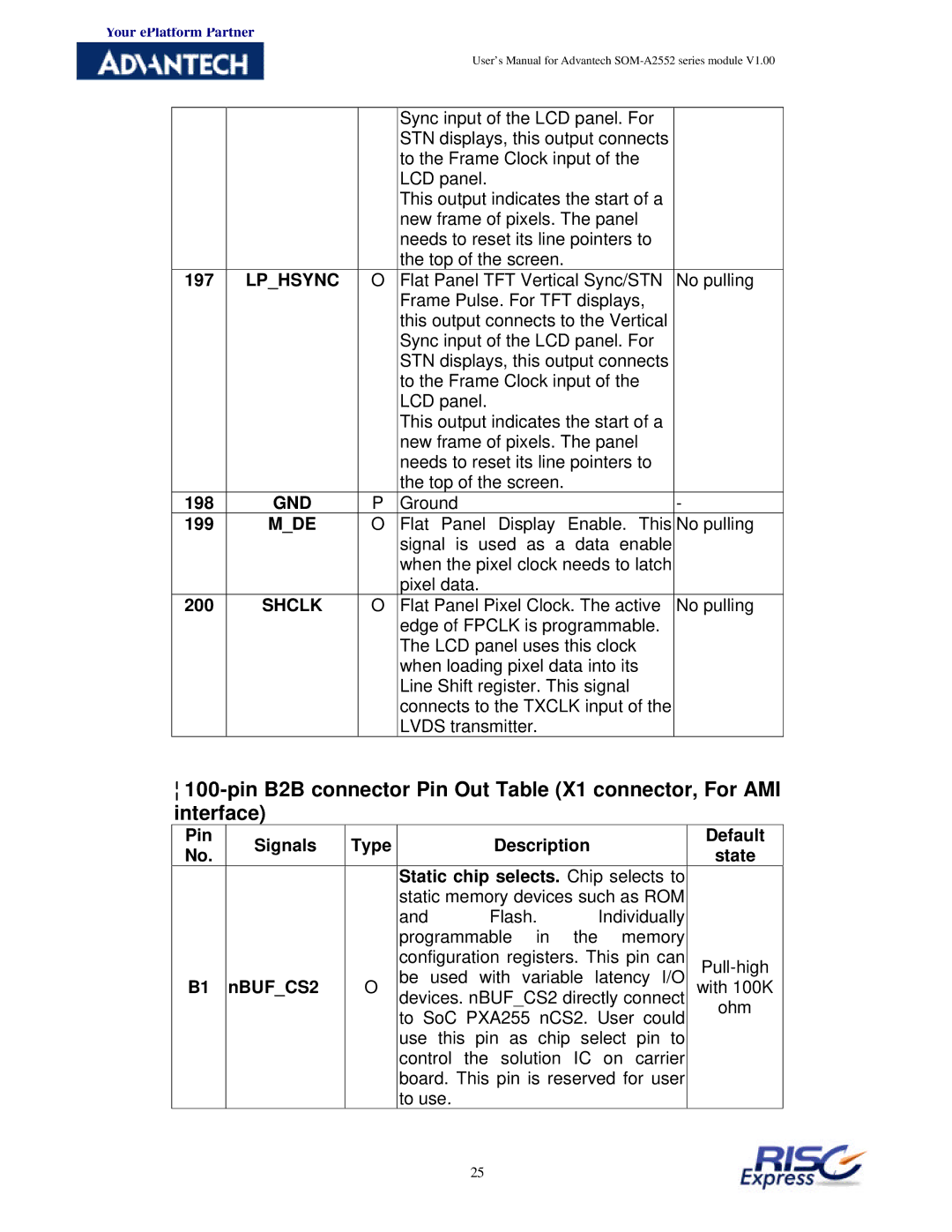
| Sync input of the LCD panel. For |
|
|
|
| STN displays, this output connects |
|
|
|
| to the Frame Clock input of the |
|
|
|
| LCD panel. |
|
|
|
| This output indicates the start of a |
|
|
|
| new frame of pixels. The panel |
|
|
|
| needs to reset its line pointers to |
|
|
|
| the top of the screen. |
|
197 | LP_HSYNC | O | Flat Panel TFT Vertical Sync/STN | No pulling |
|
|
| Frame Pulse. For TFT displays, |
|
|
|
| this output connects to the Vertical |
|
|
|
| Sync input of the LCD panel. For |
|
|
|
| STN displays, this output connects |
|
|
|
| to the Frame Clock input of the |
|
|
|
| LCD panel. |
|
|
|
| This output indicates the start of a |
|
|
|
| new frame of pixels. The panel |
|
|
|
| needs to reset its line pointers to |
|
|
|
| the top of the screen. |
|
198 | GND | P | Ground | - |
199 | M_DE | O | Flat Panel Display Enable. This | No pulling |
|
|
| signal is used as a data enable |
|
|
|
| when the pixel clock needs to latch |
|
|
|
| pixel data. |
|
200 | SHCLK | O | Flat Panel Pixel Clock. The active | No pulling |
|
|
| edge of FPCLK is programmable. |
|
|
|
| The LCD panel uses this clock |
|
|
|
| when loading pixel data into its |
|
|
|
| Line Shift register. This signal |
|
|
|
| connects to the TXCLK input of the |
|
|
|
| LVDS transmitter. |
|
Pin | Signals | Type |
| Description |
| Default |
No. |
|
| state | |||
|
|
|
|
| ||
|
|
| Static chip selects. Chip selects to |
| ||
|
|
| static memory devices such as ROM |
| ||
|
|
| and | Flash. | Individually |
|
|
|
| programmable in the | memory |
| |
|
|
| configuration registers. This pin can | |||
|
|
| be used | with variable latency I/O | ||
B1 | nBUF_CS2 | O | with 100K | |||
|
|
| devices. nBUF_CS2 directly connect | ohm | ||
|
|
| to SoC PXA255 nCS2. User could | |||
|
|
|
| |||
|
|
| use this pin as chip select pin to |
| ||
|
|
| control the solution IC on carrier |
| ||
|
|
| board. This pin is reserved for user |
| ||
|
|
| to use. |
|
|
|
25
