Your ePlatform Partner
User’s Manual for Advantech
|
|
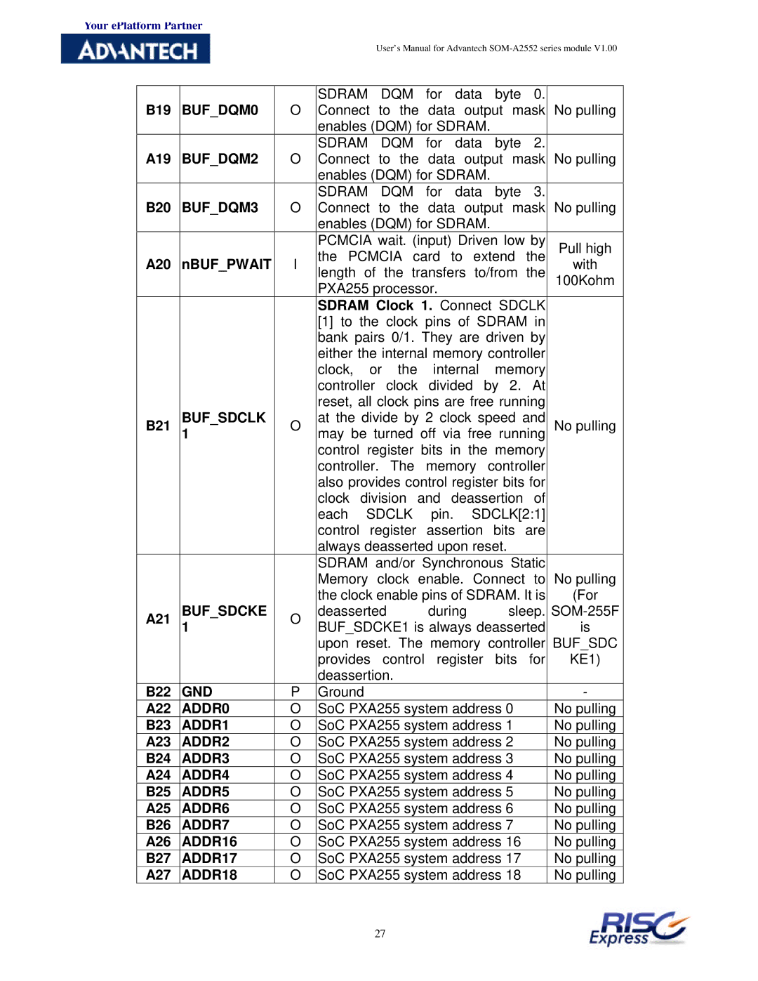
| SDRAM DQM | for | data | byte 0. |
| |
B19 | BUF_DQM0 | O | Connect to the data output mask | No pulling | ||||
|
|
| enables (DQM) for SDRAM. |
| ||||
|
|
| SDRAM DQM | for | data | byte 2. |
| |
A19 | BUF_DQM2 | O | Connect to the data output mask | No pulling | ||||
|
|
| enables (DQM) for SDRAM. |
| ||||
|
|
| SDRAM DQM | for | data | byte 3. |
| |
B20 | BUF_DQM3 | O | Connect to the data output mask | No pulling | ||||
|
|
| enables (DQM) for SDRAM. |
| ||||
|
|
| PCMCIA wait. (input) Driven low by | Pull high | ||||
|
|
| the PCMCIA card to extend the | |||||
A20 | nBUF_PWAIT | I | with | |||||
length of the transfers to/from the | ||||||||
|
|
| 100Kohm | |||||
|
|
| PXA255 processor. |
|
|
| ||
|
|
| SDRAM Clock 1. Connect SDCLK |
| ||||
|
|
| [1] to the clock pins of SDRAM in |
| ||||
|
|
| bank pairs 0/1. They are driven by |
| ||||
|
|
| either the internal memory controller |
| ||||
|
|
| clock, or the internal memory |
| ||||
|
|
| controller clock divided by 2. At |
| ||||
|
|
| reset, all clock pins are free running |
| ||||
B21 | BUF_SDCLK | O | at the divide by 2 clock speed and | No pulling | ||||
1 | may be turned off via free running | |||||||
|
|
| control register bits in the memory |
| ||||
|
|
| controller. The | memory | controller |
| ||
|
|
| also provides control register bits for |
| ||||
|
|
| clock division and deassertion of |
| ||||
|
|
| each SDCLK | pin. | SDCLK[2:1] |
| ||
|
|
| control register assertion bits are |
| ||||
|
|
| always deasserted upon reset. |
| ||||
|
|
| SDRAM and/or Synchronous Static |
| ||||
|
|
| Memory clock enable. Connect to | No pulling | ||||
|
|
| the clock enable pins of SDRAM. It is | (For | ||||
A21 | BUF_SDCKE | O | deasserted | during | sleep. | |||
1 | BUF_SDCKE1 is always deasserted | is | ||||||
|
|
| upon reset. The memory controller | BUF_SDC | ||||
|
|
| provides control register bits for | KE1) | ||||
|
|
| deassertion. |
|
|
|
| |
B22 | GND | P | Ground |
|
|
| - | |
A22 | ADDR0 | O | SoC PXA255 system address 0 | No pulling | ||||
B23 | ADDR1 | O | SoC PXA255 system address 1 | No pulling | ||||
A23 | ADDR2 | O | SoC PXA255 system address 2 | No pulling | ||||
B24 | ADDR3 | O | SoC PXA255 system address 3 | No pulling | ||||
A24 | ADDR4 | O | SoC PXA255 system address 4 | No pulling | ||||
B25 | ADDR5 | O | SoC PXA255 system address 5 | No pulling | ||||
A25 | ADDR6 | O | SoC PXA255 system address 6 | No pulling | ||||
B26 | ADDR7 | O | SoC PXA255 system address 7 | No pulling | ||||
A26 | ADDR16 | O | SoC PXA255 system address 16 | No pulling | ||||
B27 | ADDR17 | O | SoC PXA255 system address 17 | No pulling | ||||
A27 | ADDR18 | O | SoC PXA255 system address 18 | No pulling | ||||
27