Page
Page
Notebook Computer D900F
Preface
Service Manual
Preface
Trademarks
About this Manual
IMPORTANT SAFETY INSTRUCTIONS
This Computer’s Optical Device is a Laser Class 1 Product
Instructions for Care and Operation
Power Safety
5. Take care when using peripheral devices
Battery Precautions
Do not remove any batteries from the computer while it is powered on
Related Documents
VIII
Disassembly
Contents
Introduction
MXM3.0 PCI-E
Chapter 1 Introduction
Overview
1.Introduction
Introduction
System Specifications
1 - 2 System Specifications
BIOS
Processor
System Specifications 1
Power
Battery
Dimensions & Weight
1 - 4 External Locator - Top View with LCD Panel Open
External Locator - Top View with LCD Panel Open
Top View
External Locator - Front & Right side Views
External Locator - Front & Right side Views 1
Front Views
Right Side Views
External Locator - Left Side & Rear View
1 - 6 External Locator - Left Side & Rear View
Left Side View
Rear View
External Locator - Bottom View
External Locator - Bottom View 1
Bottom View
Overheating
1 - 8 Mainboard Overview - Top Key Parts
Mainboard Overview - Top Key Parts
Mainboard Top Key Parts
Mainboard Overview - Bottom Key Parts
Mainboard Overview - Bottom Key Parts 1
Mainboard Bottom
Key Parts
Mainboard Overview - Top Connectors
1 - 10 Mainboard Overview - Top Connectors
Mainboard Top Connectors
16 15
Mainboard Overview - Bottom Connectors 1
Mainboard Overview - Bottom Connectors
Mainboard Bottom Connectors
1.Introduction
Chapter 2 Disassembly
Overview
Disassembly
Overview
2.Disassembly
Maintenance Tools
Connections
2 - 2 Overview
Maintenance Precautions
Cleaning
Disassembly Steps
Removing the Battery
Removing the Battery
Battery Removal
a. Loosen screws b. Release the battery
2 - 6 Removing the Optical CD/DVD Device
Removing the Optical CD/DVD Device
Optical Device Removal
HDD Assembly Removal
Removing the Hard Disk Drive
Removing the Hard Disk Drive 2
Secondary HDD Assembly Removal
3. Hard Disk Assembly
Removing the Hard Disks in the Secondary HDD Bay
2 - 8 Removing the Hard Disk Drive
Removing the Keyboard
Keyboard Tabs
Removing the Keyboard 2
Keyboard Removal
Removing the System Memory RAM
2 - 10 Removing the System Memory RAM
Removing the System Memory RAM 2
RAM Module Removal cont’d
Upgrading a Third System Memory RAM Module
2 - 12 Removing the System Memory RAM
Third RAM Module Removal
2 Screws
Disassembly
2 - 14 Removing the Processor
Removing the Processor
Processor Removal
Removing the VGA Card
Removing the VGA Card 2
VGA Card Removal
17 Screws
2 - 16 Removing the VGA Card
VGA Card Removal cont’d
Installing the VGA Card
VGA Card Installation
2 - 18 Removing the Wireless LAN Module
Removing the Wireless LAN Module
Wireless LAN Module Removal
Removing the Bluetooth Module 2
Removing the Bluetooth Module
Bluetooth Module Removal
2 - 20 Removing the Modem
Removing the Modem
Modem Removal
Removing the TV Tuner Card 2
Removing the TV Tuner Card
TV Tuner Card Removal
2 - 22 Removing the Intel Turbo Memory Card
Removing the Intel Turbo Memory Card
Intel Turbo Memory Card Removal
A.Part Lists
Appendix A Part Lists
Part Lists
Part List Illustration Location
Table A
A - 2 Part List Illustration Location
Part List Illustration Location
Figure A
Top A
㥽䈜㾲䈷
㪾䒅 㾲䈷
Bottom
A - 4 Bottom
Bottom
㾲䈷 㾲䈷
㾲䈷 㾲䈷 㾲䈷 㾲䈷 㾲䈷 㾲䈷 㾲䈷 㾲䈷 㾲䈷 㾲䈷 㳰㛨䨑㛽㾲䈷 㾲䈷 㾲䈷 褜㬘㾲䈷 㾲䈷䐈㗱㗺㖛㟯㧹 㾲䈷 㾲䈷 褜㬘 㾲䈷
LCD A
㾲䈷䐈㗱㗺㟯㧹 㾲䈷 㺉䧰 㙰䕊㾲䈷 㾲䈷 㾲䈷 ー㞁褜㾲䈷 㾲䈷 䐥㴆㞝䧰㾲䈷 褜㬘 㾲䈷 㾲䈷 㾲䈷 褜㬘 㾲䈷 㾲䈷
Mainboard
A - 6 Mainboard
Mainboard
㾲䈷 㾲䈷 㾲䈷 㾲䈷 㾲䈷 㾲䈷 㾲䈷 䠂㖨㖃䏧 㾲䈷 㾲䈷 㗸㗺㾲䈷 㗸㗺㾲䈷
Blu-Ray Combo
Blu-Ray Combo A
Blu-Ray Combo
㾲䈷 㾲䈷 㾲䈷 㾲䈷 㾲䈷 㾲䈷
A - 8 DVD Super Multi
DVD Super Multi
DVD Super Multi
Appendix B Schematic Diagrams
B.Schematic Diagrams
Schematic Diagrams
Schematic Diagrams
System Block Diagram
CLEVO D900F System Block Diagram
B - 2 System Block Diagram
Diagram
LGA1366 Part A DDR3 1/2
LGA1366 Part A DDR3 1/2 B
Sheet 2 of LGA1366 Part A DDR3 1/2
ChannelA
LGA1366 Part B DDR3 2/2
B - 4 LGA1366 Part B DDR3 2/2
Sheet 3 of
LGA1366 Part B DDR3 2/2
B.Schematic
LGA1366 Part C QPI
Diagrams
LGA1366 Part C QPI B
LGA1366 Part C Power
B - 6 LGA1366 Part C Power
Sheet 5 of LGA1366 Part C Power
CAD NOTE
LGA1366 Part E GND, Thermal
Place near to the CPU
LGA1366 Part E GND, Thermal B
Sheet 6 of LGA1366 Part E GND, Thermal
DDR3 Channel A SO-DIMM0
ChannelA
B - 8 DDR3 Channel A SO-DIMM0
Sheet 7 of DDR3 Channel A SO-DIMM0
B.Schematic Diagrams
DDR3 Channel B SO-DIMM1
ChannelB
DDR3 Channel B SO-DIMM1 B
DDR3 Channel C SO-DIMM2
ChannelC
B - 10 DDR3 Channel C SO-DIMM2
Sheet 9 of DDR3 Channel C SO-DIMM2
X58 QPI Interface
GT/s De fault
X58 QPI Interface B
X58 QPI Interface
X58 PCIEX16, PCIEX4, DMI
B.Schematic Diagrams
PCIEX162 D900B none using now
PCIEX4 D900B none using now
X58 Misc
X58 Misc B
Sheet 12 of X58 Misc
6 OF
B - 14 X58 PWR
X58 PWR
Sheet 13 of X58 PWR
X58 GND
B.Schematic
X58 GND B
Sheet 14 of
Diagrams
B.Schematic
ICH10 DMI/PCIE/USB/SATA
POWER OK
ICH10 PCI/SPI/Other
ICH10 PCI/SPI/Other B
Sheet 16 of ICH10 PCI/SPI Other
Zo= 55O?
ICH10 Power/GND
B - 18 ICH10 Power/GND
Sheet 17 of ICH10 Power/GND
VCCHDA
Intel Debug Card & Fan Control
Schematic
Intel Debug Card & Fan Control B
Sheet 18 of
Clock Generator CV193
B - 20 Clock Generator CV193
Sheet 19 of Clock Generator CV193
SRC7..0
MXM3.0 PCI-E
Schematic Diagrams
B.SchematicDiagrams
MXM3.0 PCI-E B
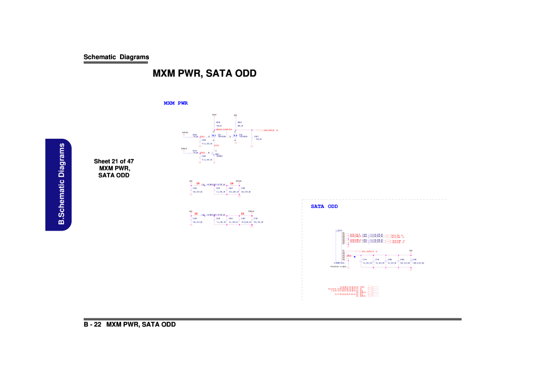
MXM PWR, SATA ODD
B - 22 MXM PWR, SATA ODD
Sheet 21 of MXM PWR, SATA ODD
MXM PWR
HDMI & e-SATA
HDMI SWITCH
HDMI & e-SATA B
HDMI
DVI-I
PLEASE CLOSE TO CONNECTOR
B - 24 DVI-I
DVI-I
Schematic
LCD, INT
0.01uF for LVDS power time
LCD, INT B
Card Reader/1394
IEEE13941394
B - 26 Card Reader/1394
Sheet 25 of Card Reader/1394
RTL8111C
Schematic Diagrams
DATASHEET? 1.2V? ? ?
Hi Enable
ALC662 / AMP TP6047A-4
B - 28 ALC662 / AMP TP6047A-4
Sheet 27 of 47 ALC662 / AMP TPA6047A4
FRONT CHANNEL 2W
KBC-ITE IT8512E
KBC-ITE IT8512E B
Sheet 28 of
KBC-ITE IT8512E
Mini WLAN/ TMP/ TPA6017A2
Disable TPM function
LPC reset timing
B - 30 Mini WLAN/ TMP/ TPA6017A2
Daughter CONN
PHONE JACK BOARD
CLICK BOARD
SWITCH BOARD
SATA HDD/ CCD/ BT/ PC BEEP
Bluetooth
B - 32 SATA HDD/ CCD/ BT/ PC BEEP
Sheet 31 of SATA HDD/ CCD BT/ PC BEEP
New Card/ MDC/ TV/ Robson
New Card/ MDC/ TV/ Robson B
New Card/ mDC
NEW CARD
Audio Board
B - 34 Audio Board
Sheet 33 of Audio Board
LINE IN
Card Reader Board B
Card Reader Board
Sheet 34 of Card Reader Board
Click Board
B - 36 Click Board
Sheet 35 of Click Board
10MIL
Hotkey Board
Hotkey Board B
Sheet 36 of Hotkey Board
SPI FLASH TOOL
Switch Board
Diagrams
B - 38 Switch Board
Sheet 37 of 47 Switch Board
USB Board
EMI solution,when placement
USB Board B
Sheet 38 of USB Board
Power CPUVTT
B - 40 Power CPUVTT
ISL6314CR POWER CKT
Sheet 39 of Power CPUVTT
Power 1.5V, 0.75VS
Power 1.5V, 0.75VS, 12V B
Power
0.75VS
Power 1.8VS, 1.1VS
B - 42 Power 1.8VS, 1.1VS
Power 1.8VS, 1.1VS
Sheet 41 of
Power ACIn, Charge
Power ACIn, Charge B
POWER
AC IN & CHARGER
Power Switch, ICH1.1VS
B - 44 Power Switch, ICH1.1VS
Power Switch
ICH1.1VS
Power VCORE
Power VCORE B
Sheet 44 of Power VCORE
NCP5392 Intel VRD11.1 POWER CKT
Power VDD3, VDD5
B - 46 Power VDD3, VDD5
Sheet 45 of Power VDD3, VDD5
VDD3,VDD5
Power Delivery Chart B
Power Delivery Chart
Sheet 46 of Power Delivery Chart
Power Sequence Diagram
B - 48 Power Sequence Diagram
Sheet 47 of Power Sequence Diagram
D900F V0.0 BOOT