CY14B101Q1
CY14B101Q2
PRELIMINARYCY14B101Q3
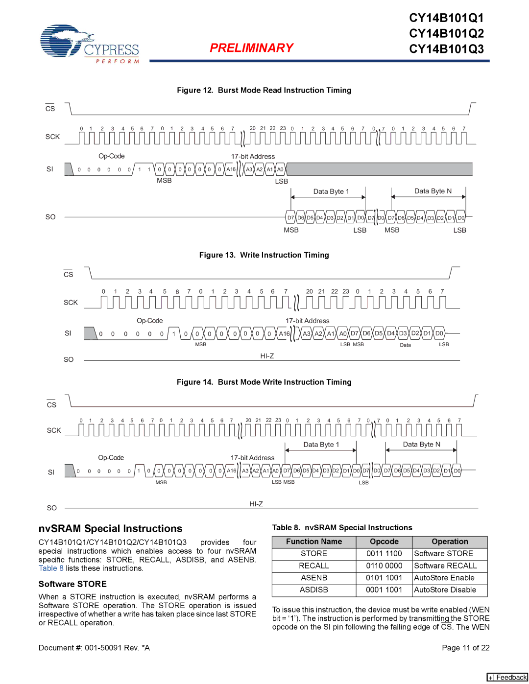
Figure 12. Burst Mode Read Instruction Timing
CS
SCK
SI
SO
0 | 1 |
| 2 | 3 | 4 | 5 | 6 | 7 | 0 | 1 | 2 | 3 | 4 | 5 | 6 | 7 |
| 20 | 21 | 22 | 23 | 0 | 1 | 2 | 3 | 4 | 5 | 6 | 7 | 0 |
| 7 | 0 | 1 | 2 | 3 | 4 | 5 | 6 | 7 |
|
|
|
|
|
|
|
|
|
|
|
|
|
|
|
|
| ~~ |
|
|
|
|
|
|
|
|
|
|
|
| ~ |
|
|
|
|
|
|
|
| ||
|
|
|
|
|
|
|
|
|
|
|
|
|
|
|
|
|
|
|
|
|
|
|
|
|
|
|
| ~ |
|
|
|
|
|
|
|
|
| |||
|
|
|
|
|
|
|
|
|
|
|
|
|
|
|
|
|
|
|
|
|
|
|
|
|
|
|
|
|
|
|
| |||||||||
0 | 0 | 0 | 0 |
| 0 | 0 | 1 | 1 | 0 | 0 | 0 | 0 | 0 | 0 | 0 | A16 |
| A3 | A2 | A1 | A0 |
|
|
|
|
|
|
|
|
|
|
|
|
|
|
|
|
|
|
|
|
|
|
|
|
|
|
|
| MSB |
|
|
|
|
| ~~ |
|
| LSB |
|
|
|
|
|
|
|
|
|
|
|
|
|
|
|
|
|
| ||||
|
|
|
|
|
|
|
|
|
|
|
|
|
|
|
|
|
|
|
|
|
|
|
|
|
|
|
|
|
|
|
|
|
|
|
| |||||
|
|
|
|
|
|
|
|
|
|
|
|
|
|
|
|
|
|
|
|
|
|
|
| Data Byte 1 |
|
|
|
|
|
|
| Data Byte N |
| |||||||
|
|
|
|
|
|
|
|
|
|
|
|
|
|
|
|
|
|
|
|
|
| D7 | D6 D5 D4 | D3 D2 | D1 D0 | D7 D0 | D7 | D6 | D5 D4 | D3 D2 | D1 D0 | |||||||||
|
|
|
|
|
|
|
|
|
|
|
|
|
|
|
|
|
|
|
|
| MSB |
|
|
|
| LSB | ~~ | MSB |
|
|
|
| LSB | |||||||
|
|
|
|
|
|
|
|
|
|
|
|
|
|
|
|
|
|
|
|
|
|
|
|
|
|
|
|
|
|
| ||||||||||
CS
SCK
SI
SO
Figure 13. Write Instruction Timing
0 | 1 | 2 | 3 | 4 | 5 | 6 | 7 | 0 | 1 | 2 | 3 | 4 | 5 | 6 | 7 | 20 | 21 | 22 | 23 | 0 | 1 | 2 | 3 | 4 | 5 | 6 | 7 |
|
|
|
|
|
|
|
|
|
|
|
|
|
|
| ~~ |
|
|
|
|
|
|
|
|
|
|
|
|
|
|
|
|
|
|
|
|
|
|
|
|
|
|
|
|
|
|
|
|
| |||||||
0 | 0 | 0 | 0 | 0 | 0 | 1 | 0 | 0 | 0 | 0 | 0 | 0 | 0 | 0 | A16 | A3 | A2 | A1 | A0 | D7 | D6 | D5 | D4 | D3 | D2 | D1 | D0 |
|
|
|
|
|
|
|
| MSB |
|
|
|
|
|
| ~ ~ |
|
|
| LSB MSB |
|
| Data |
|
| LSB | ||
|
|
|
|
|
|
|
|
|
|
|
|
|
|
|
|
|
|
|
|
|
| ||||||
|
|
|
|
|
|
|
|
|
|
|
|
|
|
|
|
|
|
|
|
|
|
|
|
|
| ||
CS
SCK
SI
SO
Figure 14. Burst Mode Write Instruction Timing
0 | 1 | 2 | 3 | 4 | 5 | 6 | 7 | 0 | 1 | 2 | 3 | 4 | 5 | 6 | 7 | 20 | 21 | 22 | 23 | 0 | 1 | 2 | 3 | 4 | 5 | 6 | 7 | 0 |
| 7 | 0 | 1 | 2 | 3 | 4 | 5 | 6 | 7 |
|
|
|
|
|
|
|
|
|
|
|
|
|
|
| ~~ |
|
|
|
|
|
|
|
|
|
|
| ~ |
|
|
|
|
|
|
|
|
| ||
|
|
|
|
|
|
|
|
|
|
|
|
|
|
|
|
|
|
|
|
|
| Data Byte 1 |
|
|
| ~ |
|
| Data Byte N |
|
| |||||||
|
|
|
|
|
|
|
|
|
|
|
|
|
|
|
|
|
|
|
|
|
|
|
|
|
|
|
|
|
|
| ||||||||
|
|
|
|
|
|
|
|
|
|
|
|
|
|
|
|
|
|
|
| ~~ |
|
|
|
|
|
|
|
|
| |||||||||
|
|
|
|
|
|
|
|
|
|
|
|
|
|
| ~ ~ |
|
|
|
| D6 D5 D4 |
|
|
|
|
|
| D6 D5 | D4 |
|
|
|
| ||||||
0 | 0 | 0 | 0 | 0 | 0 | 1 | 0 | 0 | 0 | 0 | 0 | 0 | 0 | 0 | A16 | A3 | A2 | A1 A0 | D7 | D3 D2 | D1 | D0 D7 | D0 | D7 | D3 D2 | D1 | D0 | |||||||||||
|
|
|
|
|
|
|
| MSB |
|
|
|
|
|
|
|
|
|
| LSB MSB |
|
|
|
|
| LSB |
|
|
|
|
|
|
|
|
|
| |||
nvSRAM Special Instructions
CY14B101Q1/CY14B101Q2/CY14B101Q3 provides four special instructions which enables access to four nvSRAM specific functions: STORE, RECALL, ASDISB, and ASENB. Table 8 lists these instructions.
Software STORE
When a STORE instruction is executed, nvSRAM performs a Software STORE operation. The STORE operation is issued irrespective of whether a write has taken place since last STORE or RECALL operation.
Document #:
Table 8. nvSRAM Special Instructions
Function Name | Opcode | Operation |
STORE | 0011 1100 | Software STORE |
|
|
|
RECALL | 0110 0000 | Software RECALL |
|
|
|
ASENB | 0101 1001 | AutoStore Enable |
|
|
|
ASDISB | 0001 1001 | AutoStore Disable |
|
|
|
To issue this instruction, the device must be write enabled (WEN bit = ‘1’). The instruction is performed by transmitting the STORE opcode on the SI pin following the falling edge of CS. The WEN
Page 11 of 22
[+] Feedback