CY14B101Q1
CY14B101Q2
PRELIMINARYCY14B101Q3
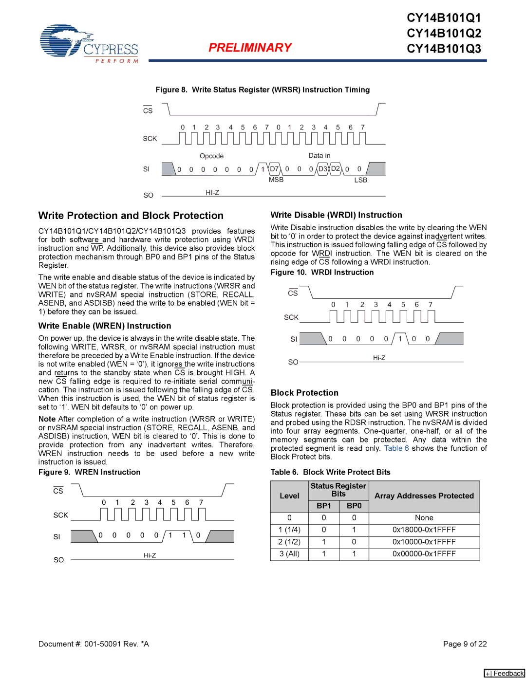
Figure 8. Write Status Register (WRSR) Instruction Timing
CS
0 1 2 3 4 5 6 7 0 1 2 3 4 5 6 7
SCK
|
|
| Opcode |
|
|
|
|
|
|
| Data in |
|
| ||
SI | 0 | 0 | 0 | 0 | 0 | 0 | 0 | 1 | D7 | 0 | 0 | 0 | D3 D2 | 0 | 0 |
|
|
|
|
|
|
|
|
| MSB |
|
|
|
|
| LSB |
SOHI-Z
Write Protection and Block Protection
CY14B101Q1/CY14B101Q2/CY14B101Q3 provides features for both software and hardware write protection using WRDI instruction and WP. Additionally, this device also provides block protection mechanism through BP0 and BP1 pins of the Status Register.
The write enable and disable status of the device is indicated by WEN bit of the status register. The write instructions (WRSR and WRITE) and nvSRAM special instruction (STORE, RECALL, ASENB, and ASDISB) need the write to be enabled (WEN bit = 1) before they can be issued.
Write Enable (WREN) Instruction
On power up, the device is always in the write disable state. The following WRITE, WRSR, or nvSRAM special instruction must therefore be preceded by a Write Enable instruction. If the device is not write enabled (WEN = ‘0’), it ignores the write instructions and returns to the standby state when CS is brought HIGH. A new CS falling edge is required to
Note After completion of a write instruction (WRSR or WRITE) or nvSRAM special instruction (STORE, RECALL, ASENB, and ASDISB) instruction, WEN bit is cleared to ‘0’. This is done to provide protection from any inadvertent writes. Therefore, WREN instruction needs to be used before a new write instruction is issued.
Figure 9. WREN Instruction
CS |
|
|
|
|
|
|
|
|
| 0 | 1 | 2 | 3 | 4 | 5 | 6 | 7 |
SCK |
|
|
|
|
|
|
|
|
SI | 0 | 0 | 0 | 0 | 0 | 1 | 1 | 0 |
SO |
|
|
|
|
|
| ||
|
|
|
|
|
|
|
| |
Write Disable (WRDI) Instruction
Write Disable instruction disables the write by clearing the WEN bit to ‘0’ in order to protect the device against inadvertent writes. This instruction is issued following falling edge of CS followed by opcode for WRDI instruction. The WEN bit is cleared on the rising edge of CS following a WRDI instruction.
Figure 10. WRDI Instruction
CS |
|
|
|
|
|
|
|
|
| 0 | 1 | 2 | 3 | 4 | 5 | 6 | 7 |
SCK |
|
|
|
|
|
|
|
|
SI | 0 | 0 | 0 | 0 | 0 | 1 | 0 | 0 |
SO |
|
|
|
|
|
| ||
|
|
|
|
|
|
|
| |
Block Protection
Block protection is provided using the BP0 and BP1 pins of the Status register. These bits can be set using WRSR instruction and probed using the RDSR instruction. The nvSRAM is divided into four array segments.
Table 6. Block Write Protect Bits
| Status Register |
| ||
Level |
| Bits | Array Addresses Protected | |
| BP1 |
| BP0 |
|
0 | 0 |
| 0 | None |
|
|
|
|
|
1 (1/4) | 0 |
| 1 | |
|
|
|
|
|
2 (1/2) | 1 |
| 0 | |
|
|
|
|
|
3 (All) | 1 |
| 1 | |
|
|
|
|
|
Document #: | Page 9 of 22 |
[+] Feedback