|
|
| CY14B101Q1 | |
|
|
| ||
|
| PRELIMINARY | CY14B101Q2 | |
|
| CY14B101Q3 | ||
|
|
|
|
|
|
|
|
|
|
Pinouts
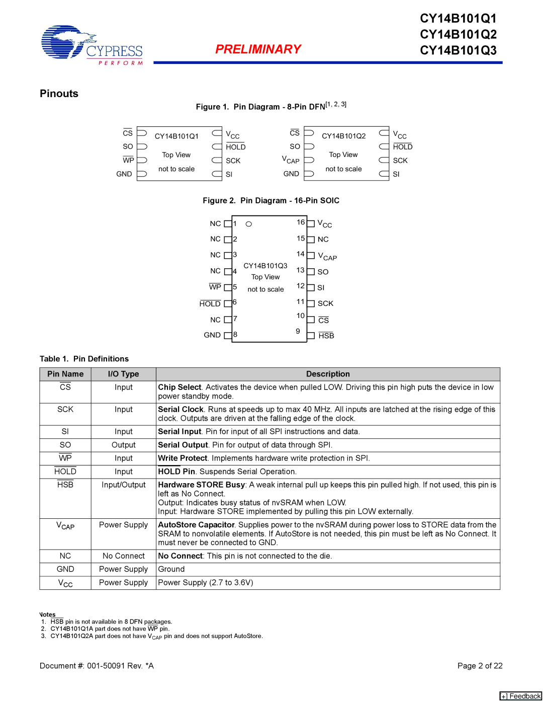
Figure 1. Pin Diagram - 8-Pin DFN[1, 2, 3]
CS | CY14B101Q1 | VCC | CS | CY14B101Q2 | VCC | |
SO | Top View | HOLD | SO | Top View | HOLD | |
WP | SCK | VCAP | SCK | |||
not to scale | not to scale | |||||
GND | SI | GND | SI | |||
|
|
Figure 2. Pin Diagram - 16-Pin SOIC
|
|
|
|
|
|
|
|
|
|
|
|
|
| NC | 1 |
| 16 | VCC | |||||
|
|
|
|
|
|
|
|
|
|
|
|
|
| NC | 2 |
| 15 | NC | |||||
|
|
|
|
|
|
|
|
|
|
|
|
|
| NC | 3 | CY14B101Q3 | 14 | VCAP | |||||
|
|
|
|
|
|
|
|
|
|
|
|
|
| NC | 4 | 13 | SO | ||||||
|
|
|
|
|
|
|
|
|
|
|
|
|
|
|
|
|
| Top View | 12 |
|
|
|
|
|
|
|
|
|
|
|
|
|
|
|
|
|
|
|
|
| 5 |
| SI | ||||
|
|
|
|
|
|
|
|
|
|
|
| WP | not to scale | ||||||||||
|
|
|
|
|
|
|
|
|
|
|
|
|
|
| 6 |
| 11 | SCK | |||||
|
|
|
|
|
|
|
|
|
|
|
| HOLD |
| ||||||||||
|
|
|
|
|
|
|
|
|
|
|
|
|
| NC | 7 |
| 10 |
|
|
|
| ||
|
|
|
|
|
|
|
|
|
|
|
|
|
|
|
| CS | |||||||
|
|
|
|
|
|
|
|
|
|
|
|
|
|
|
|
| |||||||
|
|
|
|
|
|
|
|
|
|
|
|
| GND | 8 |
| 9 |
|
|
|
| |||
|
|
|
|
|
|
|
|
|
|
|
|
|
|
| HSB | ||||||||
|
|
|
|
|
|
|
|
|
|
|
|
|
|
|
| ||||||||
Table 1. Pin Definitions |
|
|
|
|
|
|
|
|
|
|
|
|
|
| |||||||||
|
|
|
|
|
|
|
|
|
|
|
|
|
|
|
|
|
|
|
|
|
|
|
|
Pin Name | I/O Type |
|
|
|
|
|
|
|
|
|
| Description | |||||||||||
|
|
|
|
|
|
|
|
| Input |
| Chip Select. Activates the device when pulled LOW. Driving this pin high puts the device in low | ||||||||||||
|
|
|
| CS | |||||||||||||||||||
|
|
|
|
|
|
|
|
|
|
| power standby mode. |
|
|
|
|
|
| ||||||
|
| SCK | Input |
| Serial Clock. Runs at speeds up to max 40 MHz. All inputs are latched at the rising edge of this | ||||||||||||||||||
|
|
|
|
|
|
|
|
|
|
| clock. Outputs are driven at the falling edge of the clock. | ||||||||||||
|
|
|
| SI | Input |
| Serial Input. Pin for input of all SPI instructions and data. | ||||||||||||||||
|
|
|
|
|
|
|
|
|
|
|
|
|
|
|
| ||||||||
|
|
| SO | Output |
| Serial Output. Pin for output of data through SPI. | |||||||||||||||||
|
|
|
|
|
|
|
|
|
|
|
|
|
|
|
|
|
|
| |||||
|
|
|
|
|
|
|
|
| Input |
| Write Protect. Implements hardware write protection in SPI. | ||||||||||||
|
|
| WP | ||||||||||||||||||||
| HOLD |
| Input |
| HOLD | Pin. Suspends Serial Operation. |
|
|
|
| |||||||||||||
|
|
|
|
|
|
|
| Input/Output |
| Hardware STORE Busy: A weak internal pull up keeps this pin pulled high. If not used, this pin is | |||||||||||||
|
| HSB |
| ||||||||||||||||||||
|
|
|
|
|
|
|
|
|
|
| left as No Connect. |
|
|
|
|
|
|
| |||||
|
|
|
|
|
|
|
|
|
|
| Output: Indicates busy status of nvSRAM when LOW. | ||||||||||||
|
|
|
|
|
|
|
|
|
|
| Input: Hardware STORE implemented by pulling this pin LOW externally. | ||||||||||||
| VCAP | Power Supply |
| AutoStore Capacitor. Supplies power to the nvSRAM during power loss to STORE data from the | |||||||||||||||||||
|
|
|
|
|
|
|
|
|
|
| SRAM to nonvolatile elements. If AutoStore is not needed, this pin must be left as No Connect. It | ||||||||||||
|
|
|
|
|
|
|
|
|
|
| must never be connected to GND. |
|
|
|
|
| |||||||
|
|
| NC | No Connect |
| No Connect: This pin is not connected to the die. | |||||||||||||||||
|
|
|
|
|
|
|
|
|
|
|
|
|
|
| |||||||||
| GND | Power Supply | Ground |
|
|
|
|
|
|
| |||||||||||||
|
|
|
|
|
|
|
|
|
|
|
|
|
|
|
| ||||||||
|
| VCC | Power Supply |
| Power Supply (2.7 to 3.6V) |
|
|
|
|
| |||||||||||||
Notes
1.HSB pin is not available in 8 DFN packages.
2.CY14B101Q1A part does not have WP pin.
3.CY14B101Q2A part does not have VCAP pin and does not support AutoStore.
Document #: | Page 2 of 22 |
[+] Feedback