CY62137EV30

MoBL®

Capacitance (for all packages)[8]

Parameter


Description

Test Conditions


Max.


Unit

CIN


Input Capacitance

TA = 25°C, f = 1 MHz,

10


pF


VCC = VCC(typ)


COUT


Output Capacitance

10


pF

Thermal Resistance


Parameter

Description


Test Conditions


BGA

TSOP II


Unit


ΘJA

Thermal Resistance


Still Air, soldered on a 3 × 4.5 inch, two-layer


75

77


°C/W


(Junction to Ambient)[8]

printed circuit board


ΘJC

Thermal Resistance


10

13


°C/W


(Junction to Case)[8]


AC Test Loads and Waveforms

R1

VCC

OUTPUT

30 pF

INCLUDING JIG AND SCOPE


VCC


ALL INPUT PULSES


90%


10%


90%


10%

R2

GND


Rise Time = 1 V/ns


Fall Time = 1 V/ns


Equivalent to: THÉVENIN EQUIVALENT


RTH


OUTPUT


V


Parameters

2.50V

3.0V

Unit

R1

16667

1103


R2

15385

1554


RTH

8000

645

VTH

1.20

1.75

V

Data Retention Characteristics (Over the Operating Range)

Parameter

Description

Conditions

Min.

Typ.[7]

Max.

Unit

VDR

VCC for Data Retention


1


V

ICCDR

Data Retention Current

VCC= 1V


0.8

3

A


CE > VCC – 0.2V,


VIN > VCC – 0.2V or VIN < 0.2V


tCDR[8]

Chip Deselect to Data


0


ns


Retention Time


t [9]

Operation Recovery Time


t


ns

R


RC


Data Retention Waveform[10]


VCC(min)

DATA RETENTION MODE

VCC(min)

VCC

VDR > 1.5V

CE or

tCDR


tR


BHE.BLE


Notes:

8.Tested initially and after any design or process changes that may affect these parameters.

9.Full device operation requires linear VCC ramp from VDR to VCC(min.) > 100 s or stable at VCC(min.) > 100 s.

Document #: 38-05443 Rev. *B

Page 4 of 12

[+] Feedback

Page 4
Image 4
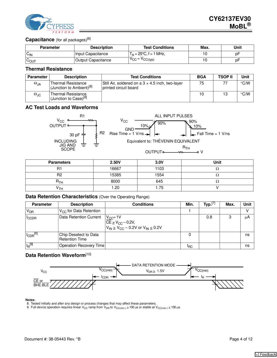
Cypress CY62137EV30 manual Thermal Resistance, AC Test Loads and Waveforms, Data Retention Waveform10, BGA Tsop

CY62137EV30 specifications

Cypress Semiconductor, a well-established name in the semiconductor industry, offers a range of memory solutions, one of which is the CY62137EV30. This product is a high-performance CMOS SRAM (Static Random Access Memory) that has gained recognition for its versatility and reliability. The CY62137EV30 is designed for various applications requiring fast access times and low power consumption.

One of the main features of the CY62137EV30 is its high-speed operation, with access times as fast as 30 ns. This capability allows the device to provide quick read and write cycles, making it suitable for applications that demand rapid data processing. The memory device operates with a voltage supply of 3.0V to 3.6V, ensuring compatibility with low-voltage digital circuits.

The device boasts a large memory capacity of 512 Kbit, organized in a 64K x 8 configuration. This structure allows for efficient data storage and retrieval, catering to applications such as telecommunications, consumer electronics, and automotive systems, where reliable data handling is crucial. The integrated memory cell design further enhances its performance, providing better speed and efficiency compared to traditional memory solutions.

Another significant characteristic of the CY62137EV30 is its low power consumption. It features a low standby current, making it ideal for battery-operated devices where power efficiency is essential. This characteristic aligns with current industry trends focusing on energy-efficient designs, contributing to longer battery life and reduced operational costs.

The CY62137EV30 also incorporates advanced technologies, such as an easy-to-use asynchronous interface. This feature simplifies the integration of the SRAM into various systems, as it allows for straightforward communication without the need for complex control signals. Additionally, the device is designed to withstand extended temperature ranges, further enhancing its reliability in diverse environmental conditions.

In summary, the Cypress CY62137EV30 stands out due to its high-speed performance, significant storage capacity, low power consumption, and ease of integration. These features make it a preferred choice for a wide range of applications, ensuring that it meets the demands of modern electronic devices and systems. As the need for efficient memory solutions continues to grow, the CY62137EV30 positions itself as a key player in the SRAM market.