CY7C027V/027VN/027AV/028V
CY7C037V/037AV/038V
Switching Characteristics Over the Operating Range[6](continued)
|
|
|
|
|
|
|
|
|
|
|
|
|
|
|
|
|
|
| CY7C027V/027VN/027AV/028V/ |
|
|
| ||||
Parameter |
|
|
|
|
|
| Description |
|
| CY7C037V/037AV/038V |
|
| Unit | |||||||||||||
|
|
|
|
|
|
|
|
| ||||||||||||||||||
|
|
|
|
|
|
|
|
|
|
|
|
|
|
|
|
|
|
|
|
| ||||||
|
|
|
|
|
|
|
|
|
|
|
|
|
|
|
|
| Min |
| Max | Min |
| Max | Min |
| Max |
|
tHD |
| Data Hold From Write End | 0 |
|
| 0 |
|
| 0 |
|
| ns | ||||||||||||||
tHZWE[9, 10] |
| R/W | LOW to High Z |
|
| 10 |
|
| 12 |
|
| 15 | ns | |||||||||||||
tLZWE[9 ,10] |
| R/W | HIGH to Low Z | 3 |
|
| 3 |
|
| 3 |
|
| ns | |||||||||||||
tWDD[36] |
| Write Pulse to Data Delay |
|
| 30 |
|
| 40 |
|
| 50 | ns | ||||||||||||||
tDDD[36] |
| Write Data Valid to Read Data Valid |
|
| 25 |
|
| 30 |
|
| 35 | ns | ||||||||||||||
Busy Timing[11] |
|
|
|
|
|
|
|
|
|
|
|
|
|
|
|
|
|
|
|
|
|
|
|
|
| |
tBLA |
| BUSY | LOW from Address Match |
|
| 15 |
|
| 20 |
|
| 20 | ns | |||||||||||||
tBHA |
| BUSY | HIGH from Address Mismatch |
|
| 15 |
|
| 20 |
|
| 20 | ns | |||||||||||||
tBLC |
| BUSY | LOW from | CE |
| LOW |
|
| 15 |
|
| 20 |
|
| 20 | ns | ||||||||||
tBHC |
| BUSY | HIGH from | CE | HIGH |
|
| 15 |
|
| 16 |
|
| 17 | ns | |||||||||||
tPS |
| Port Setup for Priority | 5 |
|
| 5 |
|
| 5 |
|
| ns | ||||||||||||||
tWB |
| R/W | HIGH after BUSY (Slave) | 0 |
|
| 0 |
|
| 0 |
|
| ns | |||||||||||||
tWH |
| R/W | HIGH after | BUSY | HIGH (Slave) | 13 |
|
| 15 |
|
| 17 |
|
| ns | |||||||||||
tBDD[13] |
| BUSY | HIGH to Data Valid |
|
| 15 |
|
| 20 |
|
| 25 | ns | |||||||||||||
Interrupt Timing[11] |
|
|
|
|
|
|
|
|
|
| ||||||||||||||||
tINS |
| INT | Set Time |
|
| 15 |
|
| 20 |
|
| 20 | ns | |||||||||||||
tINR |
| INT | Reset Time |
|
| 15 |
|
| 20 |
|
| 20 | ns | |||||||||||||
Semaphore Timing |
|
|
|
|
|
|
|
|
|
| ||||||||||||||||
tSOP |
| SEM Flag Update Pulse | (OE | or | SEM) |
| 10 |
|
| 10 |
|
| 12 |
|
| ns | ||||||||||
tSWRD |
| SEM Flag Write to Read Time | 5 |
|
| 5 |
|
| 5 |
|
| ns | ||||||||||||||
tSPS |
| SEM Flag Contention Window | 5 |
|
| 5 |
|
| 5 |
|
| ns | ||||||||||||||
tSAA |
| SEM Address Access Time |
|
| 15 |
|
| 20 |
|
| 25 | ns | ||||||||||||||
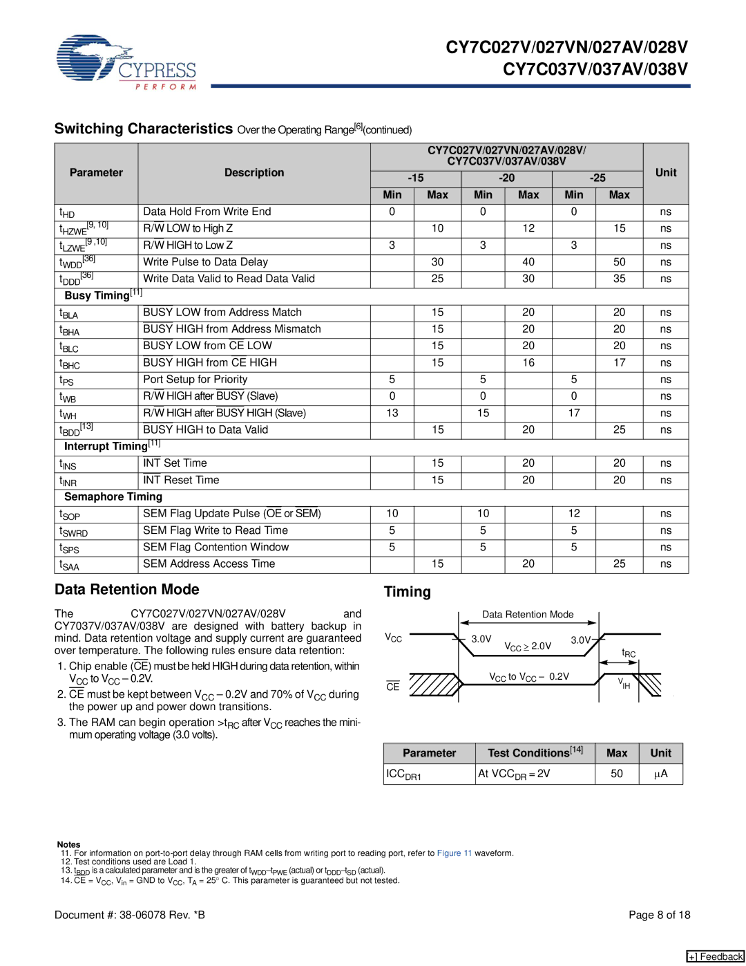
Data Retention Mode
The CY7C027V/027VN/027AV/028V and CY7037V/037AV/038V are designed with battery backup in mind. Data retention voltage and supply current are guaranteed over temperature. The following rules ensure data retention:
1.Chip enable (CE) must be held HIGH during data retention, within VCC to VCC – 0.2V.
2.CE must be kept between VCC – 0.2V and 70% of VCC during the power up and power down transitions.
Timing |
|
|
|
| Data Retention Mode | ||
VCC | 3.0V | VCC > 2.0V | 3.0V |
|
|
| |
CE | VCC to VCC – 0.2V |
| |
|
|
| |
tRC
VIH ![]()
3.The RAM can begin operation >tRC after VCC reaches the mini- mum operating voltage (3.0 volts).
Parameter | Test Conditions[14] | Max | Unit |
ICCDR1 | At VCCDR = 2V | 50 | μA |
Notes
11.For information on
12.Test conditions used are Load 1.
13.tBDD is a calculated parameter and is the greater of
14.CE = VCC, Vin = GND to VCC, TA = 25° C. This parameter is guaranteed but not tested.
Document #: | Page 8 of 18 |
[+] Feedback