|
|
|
|
|
|
|
|
|
|
|
|
|
|
|
|
| CY7C1141V18, CY7C1156V18 |
|
|
|
|
|
|
|
|
|
|
|
|
|
|
|
|
|
| CY7C1143V18, CY7C1145V18 |
|
|
|
|
|
|
|
|
|
|
|
|
|
|
|
|
|
| ||
|
|
|
|
|
|
|
|
|
|
|
|
|
|
|
| |||
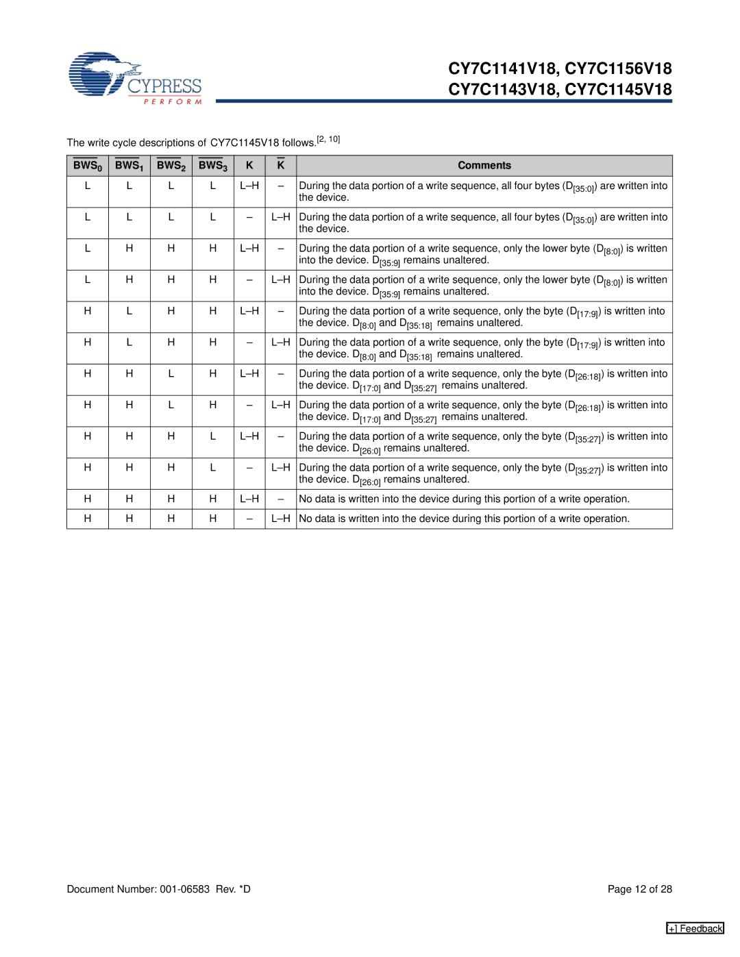
The write cycle descriptions of CY7C1145V18 follows.[2, 10] |
| |||||||||||||||||
| BWS | 0 |
| BWS | 1 |
| BWS | 2 |
| BWS | 3 | K |
| K |
| Comments |
| |
| L |
| L |
| L |
| L |
| – | During the data portion of a write sequence, all four bytes (D[35:0]) are written into |
| |||||||
|
|
|
|
|
|
|
|
|
|
|
|
|
|
|
|
| the device. |
|
| L |
| L |
| L |
| L | – | During the data portion of a write sequence, all four bytes (D[35:0]) are written into |
| ||||||||
|
|
|
|
|
|
|
|
|
|
|
|
|
|
|
|
| the device. |
|
|
|
|
|
|
|
|
|
|
|
|
|
| ||||||
| L |
| H |
| H |
| H |
| – | During the data portion of a write sequence, only the lower byte (D[8:0]) is written |
| |||||||
|
|
|
|
|
|
|
|
|
|
|
|
|
|
|
|
| into the device. D[35:9] remains unaltered. |
|
| L |
| H |
| H |
| H | – | During the data portion of a write sequence, only the lower byte (D[8:0]) is written |
| ||||||||
|
|
|
|
|
|
|
|
|
|
|
|
|
|
|
|
| into the device. D[35:9] remains unaltered. |
|
| H |
| L |
| H |
| H |
| – | During the data portion of a write sequence, only the byte (D[17:9]) is written into |
| |||||||
|
|
|
|
|
|
|
|
|
|
|
|
|
|
|
|
| the device. D[8:0] and D[35:18] remains unaltered. |
|
| H |
| L |
| H |
| H | – | During the data portion of a write sequence, only the byte (D[17:9]) is written into |
| ||||||||
|
|
|
|
|
|
|
|
|
|
|
|
|
|
|
|
| the device. D[8:0] and D[35:18] remains unaltered. |
|
| H |
| H |
| L |
| H |
| – | During the data portion of a write sequence, only the byte (D[26:18]) is written into |
| |||||||
|
|
|
|
|
|
|
|
|
|
|
|
|
|
|
|
| the device. D[17:0] and D[35:27] remains unaltered. |
|
| H |
| H |
| L |
| H | – | During the data portion of a write sequence, only the byte (D[26:18]) is written into |
| ||||||||
|
|
|
|
|
|
|
|
|
|
|
|
|
|
|
|
| the device. D[17:0] and D[35:27] remains unaltered. |
|
| H |
| H |
| H |
| L |
| – | During the data portion of a write sequence, only the byte (D[35:27]) is written into |
| |||||||
|
|
|
|
|
|
|
|
|
|
|
|
|
|
|
|
| the device. D[26:0] remains unaltered. |
|
| H |
| H |
| H |
| L | – | During the data portion of a write sequence, only the byte (D[35:27]) is written into |
| ||||||||
|
|
|
|
|
|
|
|
|
|
|
|
|
|
|
|
| the device. D[26:0] remains unaltered. |
|
| H |
| H |
| H |
| H |
| – | No data is written into the device during this portion of a write operation. |
| |||||||
|
|
|
|
|
|
|
|
|
|
|
| |||||||
| H |
| H |
| H |
| H | – | No data is written into the device during this portion of a write operation. |
| ||||||||
|
|
|
|
|
|
|
|
|
|
|
|
|
|
|
|
|
|
|
Document Number: | Page 12 of 28 |
[+] Feedback