CY7C1141V18, CY7C1156V18
CY7C1143V18, CY7C1145V18
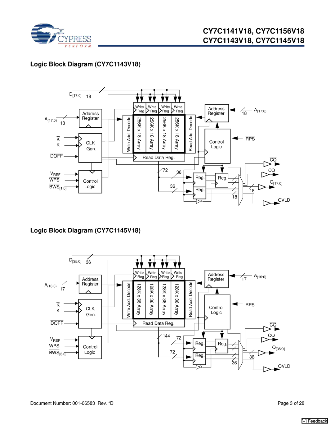
Logic Block Diagram (CY7C1143V18)
|
|
|
|
|
|
|
|
|
|
| D[17:0] | 18 |
|
| |||||||
|
|
|
|
|
|
|
|
|
|
|
|
| |||||||||
|
|
|
|
|
|
|
|
|
|
|
|
|
|
|
|
|
|
|
|
|
|
|
|
|
|
|
|
|
|
|
|
|
|
|
|
|
|
|
| Address |
| ||
|
|
|
|
|
|
|
|
|
|
|
|
|
|
|
|
|
| Register |
| ||
A(17:0) 18 |
|
| |||||||||||||||||||
|
|
|
|
| |||||||||||||||||
|
|
|
|
|
|
|
|
|
|
|
|
|
|
|
|
|
|
|
|
|
|
|
|
|
|
|
|
|
|
|
|
|
|
|
|
|
|
|
|
| |||
|
|
| K |
| CLK |
| |||||||||||||||
|
|
|
|
|
|
|
|
|
|
|
|
|
|
|
| ||||||
|
|
| K |
|
|
|
|
|
|
|
|
| |||||||||
|
|
|
|
|
|
|
|
|
| Gen. |
| ||||||||||
|
|
|
|
|
|
|
|
|
|
|
|
|
|
|
|
|
|
| |||
|
|
|
|
|
|
|
|
|
|
| |||||||||||
|
| DOFF |
|
|
|
|
|
|
|
|
|
| |||||||||
|
|
|
|
|
|
| |||||||||||||||
|
| VREF |
|
|
|
|
|
|
|
|
|
|
|
|
| ||||||
|
|
|
|
|
|
|
|
|
|
| |||||||||||
|
|
|
|
|
|
|
|
|
| ||||||||||||
|
|
|
|
|
|
|
| ||||||||||||||
| WPS |
|
|
|
|
|
|
|
|
| Control |
| |||||||||
|
|
|
|
| |||||||||||||||||
| BWS |
|
|
|
|
|
|
|
| Logic |
| ||||||||||
| [1:0] |
|
|
|
| ||||||||||||||||
|
|
|
|
|
|
|
|
|
|
|
|
|
|
|
|
|
|
|
|
|
|
|
|
| Write | Write | Write |
| Write |
|
|
|
|
|
|
|
|
|
|
|
|
|
|
|
|
|
|
|
| |
|
|
|
|
|
|
|
|
|
|
|
|
| Address |
|
|
| ||||||||||||
|
|
| Reg | Reg | Reg |
| Reg |
|
|
|
|
|
|
|
|
| Register |
|
|
| ||||||||
|
|
|
|
|
|
|
|
|
|
|
|
|
|
|
|
|
|
|
|
| ||||||||
|
| Decode | 256K x | 256K x | 256K x |
| 256K x |
| Decode |
|
|
|
|
|
|
|
|
|
|
|
|
|
|
|
| |||
|
|
|
|
|
|
|
|
|
|
|
|
|
|
|
|
|
|
| ||||||||||
|
|
|
|
|
|
|
|
|
|
|
|
|
|
|
|
|
|
| ||||||||||
|
| WriteAdd. | 18Array | 18Array | 18Array |
| 18Array |
| ReadAdd. |
|
|
|
|
|
|
| Logic |
|
| |||||||||
|
|
|
|
|
|
|
|
|
|
|
|
|
|
|
|
|
|
| Control |
|
| |||||||
|
|
| Read Data Reg. |
|
|
|
|
|
|
|
|
|
|
|
|
|
|
|
|
|
|
|
| |||||
|
|
|
|
|
|
|
|
|
|
|
|
|
|
|
|
|
|
|
|
|
|
|
|
|
|
|
|
|
|
|
|
|
| 72 | 36 |
|
|
|
|
|
|
|
|
|
|
|
|
|
|
|
|
|
|
|
|
| |
|
|
|
|
|
|
|
|
|
|
|
|
|
|
|
|
|
|
|
|
|
|
|
|
|
| |||
|
|
|
|
|
|
|
|
|
|
|
|
|
|
|
|
|
|
|
|
|
|
|
|
|
| |||
|
|
|
|
|
|
|
|
|
|
| Reg. |
|
|
|
|
|
| Reg. |
|
|
|
| ||||||
|
|
|
|
|
|
|
|
|
|
|
|
|
|
|
|
|
|
|
|
|
| |||||||
|
|
|
|
|
| 36 |
|
|
|
|
|
|
|
| ||||||||||||||
|
|
|
|
|
|
|
|
|
|
|
|
|
|
|
|
|
|
|
|
| ||||||||
|
|
|
|
|
|
|
|
|
|
|
|
|
|
|
|
|
|
|
|
|
|
|
|
|
|
| ||
|
|
|
|
|
|
|
|
|
|
|
|
|
|
|
|
|
|
|
|
|
|
|
|
|
|
| ||
|
|
|
|
|
|
|
|
|
|
|
|
|
|
|
|
|
|
|
|
|
|
|
|
|
|
| ||
|
|
|
|
|
|
|
|
|
| Reg. |
|
|
|
|
|
|
|
|
|
|
|
| ||||||
|
|
|
|
|
|
|
|
|
|
|
|
|
|
|
|
|
|
|
|
|
|
|
|
| ||||
18
18A(17:0)
RPS
CQ
CQ
Q[17:0]
18
QVLD
Logic Block Diagram (CY7C1145V18)
|
|
|
|
|
|
|
|
|
|
| D[35:0] | 36 |
|
| |||||||
|
|
|
|
|
|
|
|
|
|
|
|
| |||||||||
|
|
|
|
|
|
|
|
|
|
|
|
|
|
|
|
|
|
|
|
|
|
|
|
|
|
|
|
|
|
|
|
|
|
|
|
|
|
|
| Address |
| ||
|
|
|
|
|
|
|
|
|
|
|
|
|
|
|
|
|
| Register |
| ||
A(16:0) 17 |
|
| |||||||||||||||||||
|
|
|
|
| |||||||||||||||||
|
|
|
|
|
|
|
|
|
|
|
|
|
|
|
|
|
|
|
|
|
|
|
|
|
|
|
|
|
|
|
|
|
|
|
|
|
|
|
|
| |||
|
|
| K |
| CLK |
| |||||||||||||||
|
|
|
|
|
|
|
|
|
|
|
|
|
|
|
| ||||||
|
|
| K |
|
|
|
|
|
|
|
|
| |||||||||
|
|
|
|
|
|
|
|
|
| Gen. |
| ||||||||||
|
|
|
|
|
|
|
|
|
|
|
|
|
|
|
|
|
|
| |||
|
|
|
|
|
|
|
|
|
|
| |||||||||||
|
| DOFF |
|
|
|
|
|
|
|
|
|
| |||||||||
|
|
|
|
|
|
| |||||||||||||||
| VREF |
|
|
|
|
|
|
|
|
|
|
|
|
|
| ||||||
|
|
|
|
|
|
|
|
|
|
|
| ||||||||||
|
|
|
|
|
|
|
|
|
| ||||||||||||
|
|
|
|
|
|
|
| ||||||||||||||
| WPS |
|
|
|
|
|
|
|
|
| Control |
| |||||||||
|
|
|
|
| |||||||||||||||||
| BWS |
|
|
|
|
|
|
|
| Logic |
| ||||||||||
| [3:0] |
|
|
|
| ||||||||||||||||
|
|
|
|
|
|
|
|
|
|
|
|
|
|
|
|
|
|
|
|
|
|
|
|
| Write | Write | Write | Write |
|
|
|
|
|
|
|
|
|
|
|
|
|
|
|
|
|
|
|
| |
|
|
|
|
|
|
|
|
|
|
|
| Address |
|
|
| ||||||||||||
|
|
| Reg | Reg | Reg | Reg |
|
|
|
|
|
|
|
|
| Register |
|
|
| ||||||||
|
| Decode | 128K x | 128K x | 128K x | 128K x |
| Decode |
|
|
|
|
|
|
|
|
|
|
|
|
|
|
|
| |||
|
|
|
|
|
|
|
|
|
|
|
|
|
|
|
|
|
|
| |||||||||
|
|
|
|
|
|
|
|
|
|
|
|
|
|
|
|
|
|
| |||||||||
|
| WriteAdd. | 36Array | 36Array | 36Array | 36Array |
| ReadAdd. |
|
|
|
|
|
|
| Logic |
|
| |||||||||
|
|
|
|
|
|
|
|
|
|
|
|
|
|
|
|
|
| Control |
|
| |||||||
|
|
| Read Data Reg. |
|
|
|
|
|
|
|
|
|
|
|
|
|
|
|
|
|
|
|
| ||||
|
|
|
|
|
|
|
|
|
|
|
|
|
|
|
|
|
|
|
|
|
|
|
|
|
|
|
|
|
|
|
|
| 144 | 72 |
|
|
|
|
|
|
|
|
|
|
|
|
|
|
|
|
|
|
|
|
|
|
|
|
|
|
|
|
|
|
|
|
|
|
|
|
|
|
|
|
|
|
|
|
|
|
| ||
|
|
|
|
|
|
|
|
|
|
|
|
|
|
|
|
|
|
|
|
|
|
|
|
|
| ||
|
|
|
|
|
|
|
|
|
|
| Reg. |
|
|
|
|
|
| Reg. |
|
|
|
| |||||
|
|
|
|
|
|
|
|
|
|
|
|
|
|
|
|
|
|
|
|
| |||||||
|
|
|
|
| 72 |
|
|
|
|
|
|
|
| ||||||||||||||
|
|
|
|
|
|
|
|
|
|
|
|
|
|
|
|
|
|
|
| ||||||||
|
|
|
|
|
|
|
|
|
|
|
|
|
|
|
|
|
|
|
|
|
|
|
|
|
| ||
|
|
|
|
|
|
|
|
|
|
|
|
|
|
|
|
|
|
|
|
|
|
|
|
|
| ||
|
|
|
|
|
|
|
|
|
|
|
|
|
|
|
|
|
|
|
|
|
|
|
|
|
| ||
|
|
|
|
|
|
|
|
| Reg. |
|
|
|
|
|
|
|
|
|
|
|
| ||||||
|
|
|
|
|
|
|
|
|
|
|
|
|
|
|
|
|
|
|
|
|
|
|
| ||||
36
17A(16:0)
RPS
CQ
CQ
Q[35:0]
36
QVLD
Document Number: | Page 3 of 28 |
[+] Feedback