CY7C1146V18, CY7C1157V18
CY7C1148V18, CY7C1150V18
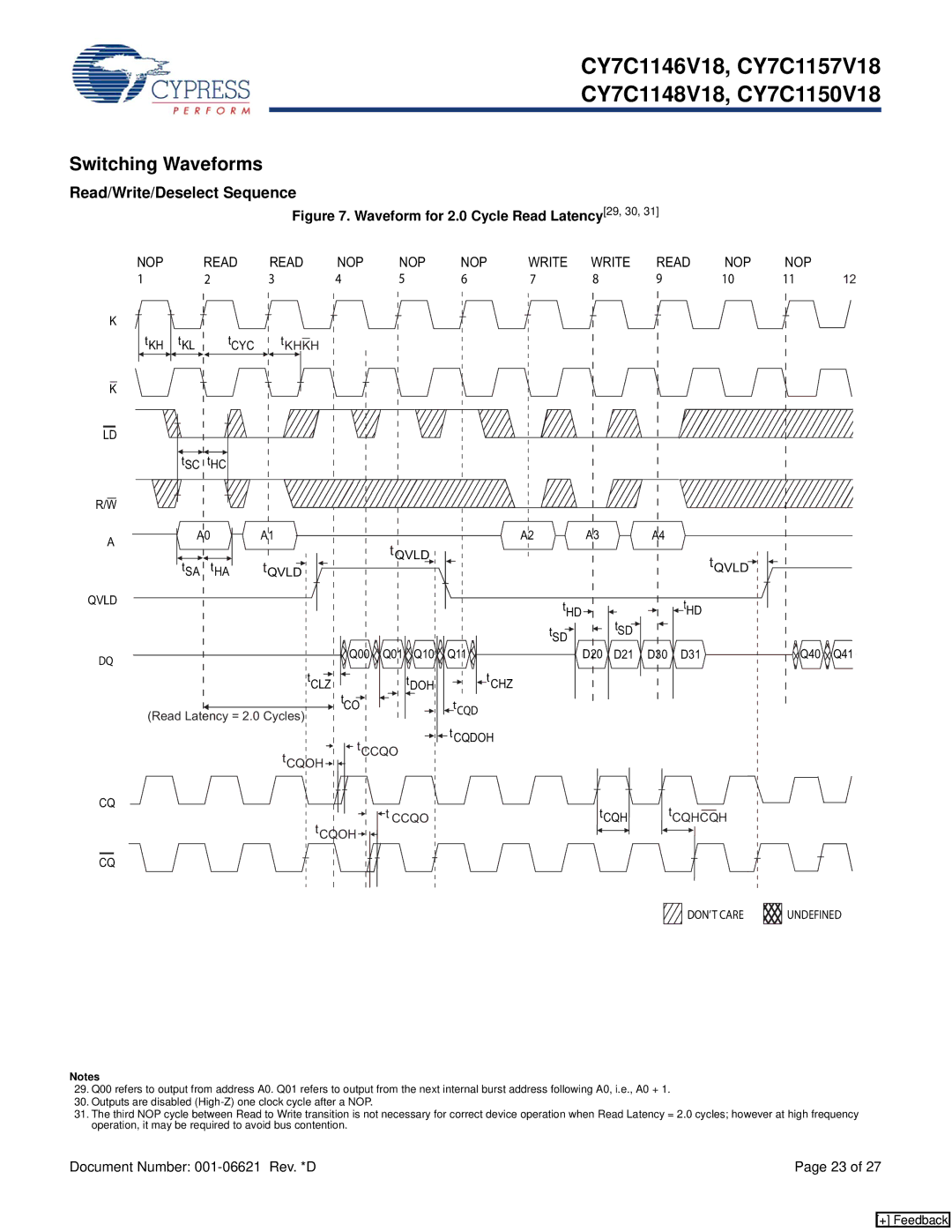
Switching Waveforms
Read/Write/Deselect Sequence
Figure 7. Waveform for 2.0 Cycle Read Latency[29, 30, 31]
NOP
1
K
tKH
| READ | READ | NOP | NOP | NOP | WRITE | WRITE | READ | NOP | NOP |
|
| 2 | 3 | 4 | 5 | 6 | 7 | 8 | 9 | 10 | 11 | 12 |
tKL | tCYC | tKHKH |
|
|
|
|
|
|
|
|
|
K
LD ![]() tSC tHC
tSC tHC
R/W
A | A0 | A1 |
| A2 | A3 | A4 |
|
|
|
|
|
|
|
| |
| tSA tHA | tQVLD |
|
|
| tQVLD |
|
QVLD |
|
|
|
| tHD | tHD |
|
|
|
|
|
|
| ||
|
|
|
|
| tSD |
|
|
DQ |
| Q00 | Q01 Q10 | Q11 | D21 | D30 D31 | Q40 Q41 |
|
|
|
|
|
|
| |
|
| tCLZ | tDOH | tCHZ |
|
|
|
|
| tCO |
| tCQD |
|
|
|
| (Read Latency = 2.0 Cycles) |
|
|
|
|
| |
|
| tCCQO | tCQDOH |
|
|
| |
|
| tCQOH |
|
|
|
|
|
CQ |
|
| t CCQO |
| tCQH | tCQHCQH |
|
|
| tCQOH |
|
| |||
|
|
|
|
|
|
| |
CQ |
|
|
|
|
|
|
|
|
|
|
|
|
| DON’T CARE | UNDEFINED |
Notes
29.Q00 refers to output from address A0. Q01 refers to output from the next internal burst address following A0, i.e., A0 + 1.
30.Outputs are disabled
31.The third NOP cycle between Read to Write transition is not necessary for correct device operation when Read Latency = 2.0 cycles; however at high frequency operation, it may be required to avoid bus contention.
Document Number: | Page 23 of 27 |
[+] Feedback