
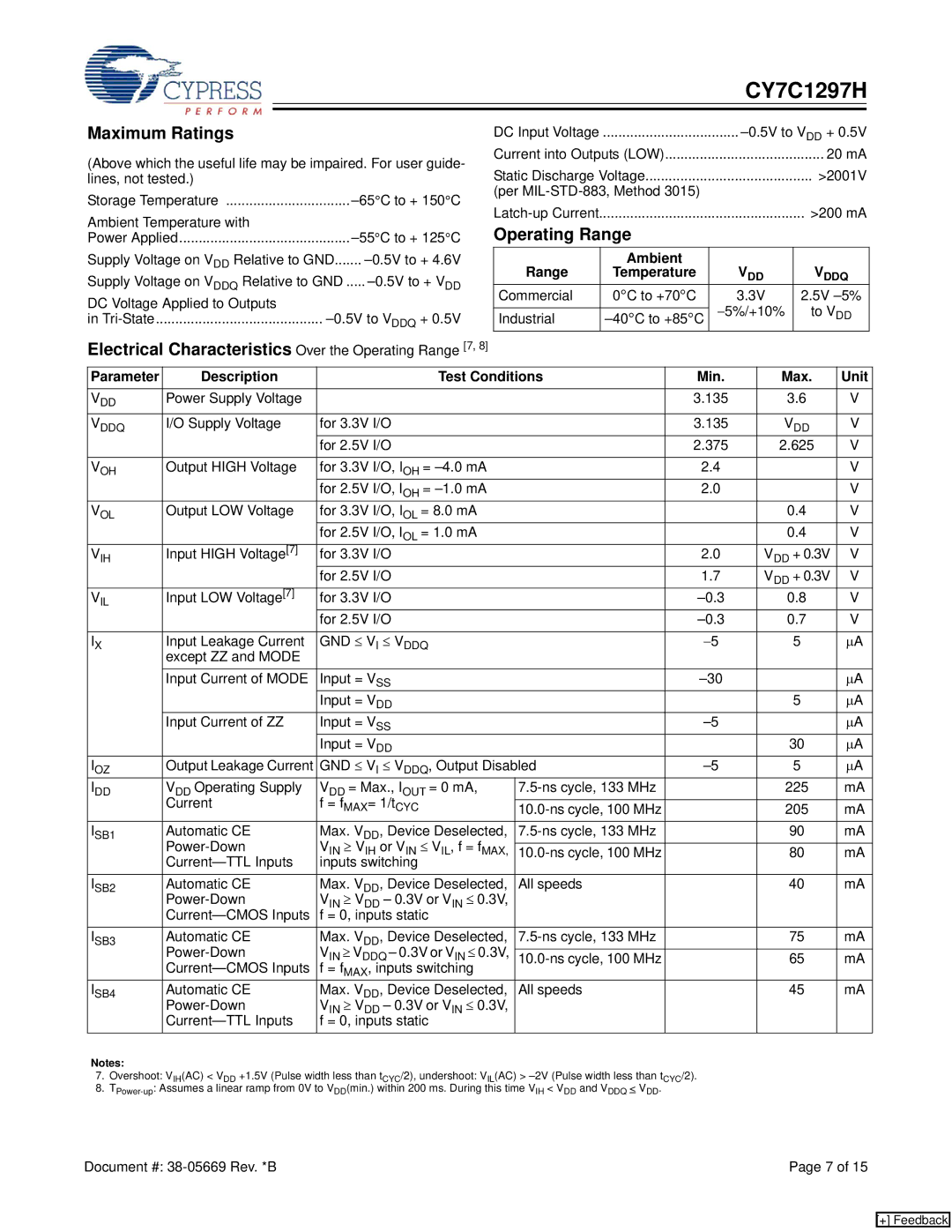
CY7C1297H specifications
The Cypress CY7C1297H is a high-performance synchronous static random-access memory (SRAM) that offers an optimal solution for various memory applications, particularly in communication and networking devices. Designed as a part of the Cypress family of SRAMs, the CY7C1297H encompasses advanced features that significantly enhance its performance and efficiency.One of the standout features of the CY7C1297H is its high density, providing 128 megabits of storage capacity. This ample memory size allows it to support a wide range of applications, especially in complex systems where large data buffers are crucial. The architecture is built on advanced CMOS technology, ensuring low power consumption and high speed. The device operates at frequencies up to 166 MHz, enabling fast data access and processing, which is vital for high-speed networking applications.
The CY7C1297H SRAM also supports synchronous interface, ensuring that data transfers are synchronized with clock cycles, thus eliminating delays associated with asynchronous memory types. This synchronous operation enhances the performance of high-speed systems by reducing cycle time and increasing throughput. The device utilizes a burst mode feature, allowing for sequential data access without the need for repeated address inputs, which further boosts efficiency during data retrieval.
Additionally, the CY7C1297H comes with an advanced write operation capability, including features such as byte-write and latch control, enabling partial updates and reducing system overhead. This flexibility is especially beneficial for applications requiring dynamic memory updates such as packet processing and buffering in sophisticated communication environments.
In terms of power management, the CY7C1297H is designed with low standby and active power consumption characteristics. This not only contributes to lower energy costs but also extends the lifespan of the device, making it suitable for battery-operated systems.
The package options for the CY7C1297H are diverse, allowing for easy integration into various designs. It is available in both leaded and lead-free versions, catering to various environmental and regulatory requirements.
In summary, the Cypress CY7C1297H SRAM is a high-density, high-speed memory solution that excels in synchronous operation, low power consumption, and advanced features such as burst mode access and flexible write capabilities. Its robust performance makes it a top choice for applications in telecommunications, networking, and other data-intensive environments, paving the way for next-generation memory solutions.