CY7C1297H

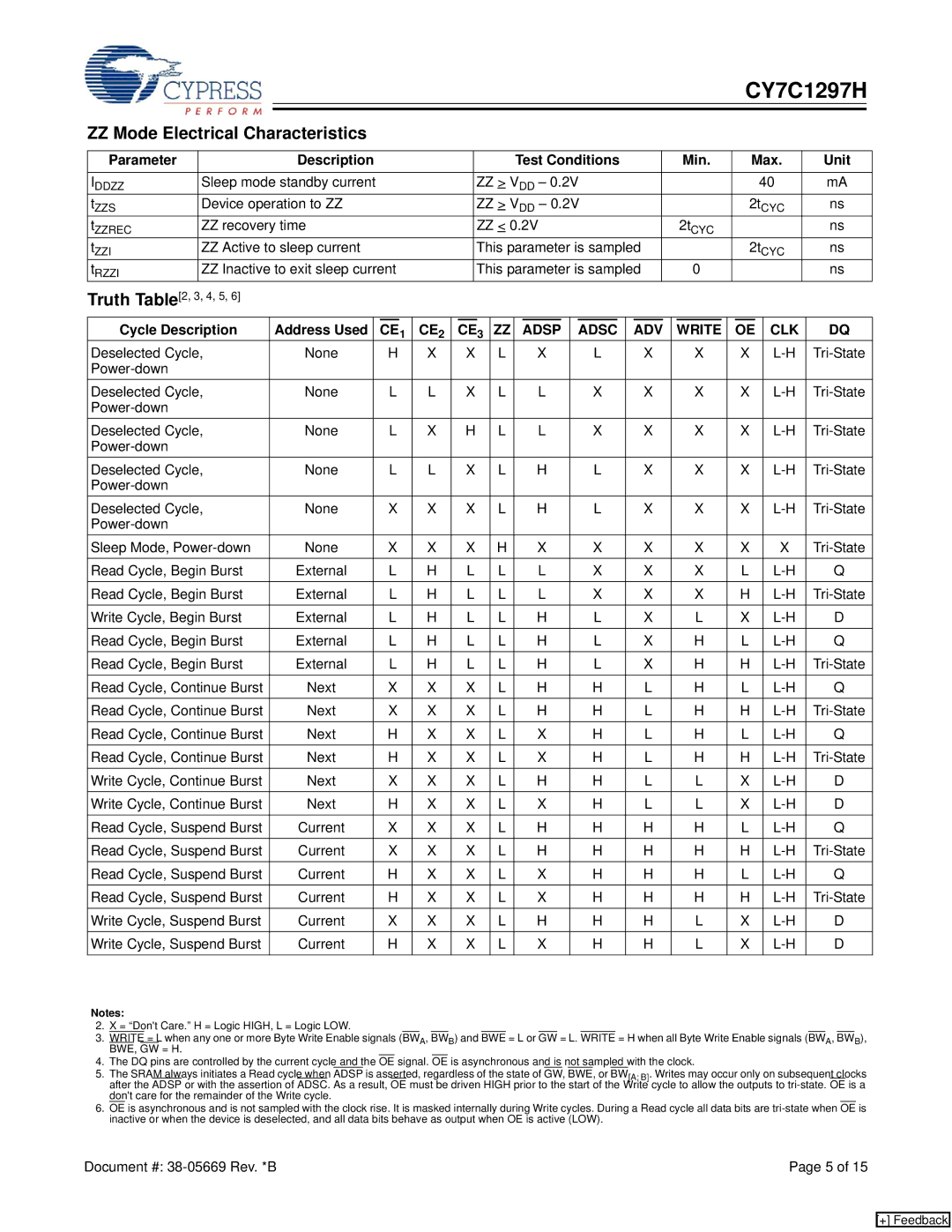
ZZ Mode Electrical Characteristics

Parameter

Description

Test Conditions

Min.

Max.

Unit

IDDZZ

Sleep mode standby current

ZZ > VDD – 0.2V


40

mA

tZZS

Device operation to ZZ

ZZ > VDD – 0.2V


2tCYC

ns

tZZREC

ZZ recovery time

ZZ < 0.2V

2tCYC


ns

tZZI

ZZ Active to sleep current

This parameter is sampled


2tCYC

ns

tRZZI

ZZ Inactive to exit sleep current

This parameter is sampled

0


ns

Truth Table[2, 3, 4, 5, 6]

Cycle Description

Address Used

CE1

CE2

CE3

ZZ

ADSP

ADSC

ADV

WRITE

OE

CLK

DQ

Deselected Cycle,

None

H

X

X

L

X

L

X

X

X

L-H

Tri-State

Power-down


Deselected Cycle,

None

L

L

X

L

L

X

X

X

X

L-H

Tri-State

Power-down


Deselected Cycle,

None

L

X

H

L

L

X

X

X

X

L-H

Tri-State

Power-down


Deselected Cycle,

None

L

L

X

L

H

L

X

X

X

L-H

Tri-State

Power-down


Deselected Cycle,

None

X

X

X

L

H

L

X

X

X

L-H

Tri-State

Power-down


Sleep Mode, Power-down

None

X

X

X

H

X

X

X

X

X

X

Tri-State

Read Cycle, Begin Burst

External

L

H

L

L

L

X

X

X

L

L-H

Q

Read Cycle, Begin Burst

External

L

H

L

L

L

X

X

X

H

L-H

Tri-State

Write Cycle, Begin Burst

External

L

H

L

L

H

L

X

L

X

L-H

D

Read Cycle, Begin Burst

External

L

H

L

L

H

L

X

H

L

L-H

Q

Read Cycle, Begin Burst

External

L

H

L

L

H

L

X

H

H

L-H

Tri-State

Read Cycle, Continue Burst

Next

X

X

X

L

H

H

L

H

L

L-H

Q

Read Cycle, Continue Burst

Next

X

X

X

L

H

H

L

H

H

L-H

Tri-State

Read Cycle, Continue Burst

Next

H

X

X

L

X

H

L

H

L

L-H

Q

Read Cycle, Continue Burst

Next

H

X

X

L

X

H

L

H

H

L-H

Tri-State

Write Cycle, Continue Burst

Next

X

X

X

L

H

H

L

L

X

L-H

D

Write Cycle, Continue Burst

Next

H

X

X

L

X

H

L

L

X

L-H

D

Read Cycle, Suspend Burst

Current

X

X

X

L

H

H

H

H

L

L-H

Q

Read Cycle, Suspend Burst

Current

X

X

X

L

H

H

H

H

H

L-H

Tri-State

Read Cycle, Suspend Burst

Current

H

X

X

L

X

H

H

H

L

L-H

Q

Read Cycle, Suspend Burst

Current

H

X

X

L

X

H

H

H

H

L-H

Tri-State

Write Cycle, Suspend Burst

Current

X

X

X

L

H

H

H

L

X

L-H

D

Write Cycle, Suspend Burst

Current

H

X

X

L

X

H

H

L

X

L-H

D

Notes:

2.X = “Don't Care.” H = Logic HIGH, L = Logic LOW.

3.WRITE = L when any one or more Byte Write Enable signals (BWA, BWB) and BWE = L or GW = L. WRITE = H when all Byte Write Enable signals (BWA, BWB), BWE, GW = H.

4.The DQ pins are controlled by the current cycle and the OE signal. OE is asynchronous and is not sampled with the clock.

5.The SRAM always initiates a Read cycle when ADSP is asserted, regardless of the state of GW, BWE, or BW[A: B]. Writes may occur only on subsequent clocks after the ADSP or with the assertion of ADSC. As a result, OE must be driven HIGH prior to the start of the Write cycle to allow the outputs to tri-state. OE is a don't care for the remainder of the Write cycle.

6.OE is asynchronous and is not sampled with the clock rise. It is masked internally during Write cycles. During a Read cycle all data bits are tri-state when OE is inactive or when the device is deselected, and all data bits behave as output when OE is active (LOW).

Document #: 38-05669 Rev. *B

Page 5 of 15

[+] Feedback

Page 5
Image 5
Cypress CY7C1297H manual ZZ Mode Electrical Characteristics, Parameter Description Test Conditions Min Max Unit

CY7C1297H specifications

The Cypress CY7C1297H is a high-performance synchronous static random-access memory (SRAM) that offers an optimal solution for various memory applications, particularly in communication and networking devices. Designed as a part of the Cypress family of SRAMs, the CY7C1297H encompasses advanced features that significantly enhance its performance and efficiency.

One of the standout features of the CY7C1297H is its high density, providing 128 megabits of storage capacity. This ample memory size allows it to support a wide range of applications, especially in complex systems where large data buffers are crucial. The architecture is built on advanced CMOS technology, ensuring low power consumption and high speed. The device operates at frequencies up to 166 MHz, enabling fast data access and processing, which is vital for high-speed networking applications.

The CY7C1297H SRAM also supports synchronous interface, ensuring that data transfers are synchronized with clock cycles, thus eliminating delays associated with asynchronous memory types. This synchronous operation enhances the performance of high-speed systems by reducing cycle time and increasing throughput. The device utilizes a burst mode feature, allowing for sequential data access without the need for repeated address inputs, which further boosts efficiency during data retrieval.

Additionally, the CY7C1297H comes with an advanced write operation capability, including features such as byte-write and latch control, enabling partial updates and reducing system overhead. This flexibility is especially beneficial for applications requiring dynamic memory updates such as packet processing and buffering in sophisticated communication environments.

In terms of power management, the CY7C1297H is designed with low standby and active power consumption characteristics. This not only contributes to lower energy costs but also extends the lifespan of the device, making it suitable for battery-operated systems.

The package options for the CY7C1297H are diverse, allowing for easy integration into various designs. It is available in both leaded and lead-free versions, catering to various environmental and regulatory requirements.

In summary, the Cypress CY7C1297H SRAM is a high-density, high-speed memory solution that excels in synchronous operation, low power consumption, and advanced features such as burst mode access and flexible write capabilities. Its robust performance makes it a top choice for applications in telecommunications, networking, and other data-intensive environments, paving the way for next-generation memory solutions.