CY7C1310AV18
CY7C1312AV18
PRELIMINARYCY7C1314AV18
18-Mb QDR™-II SRAM 2-Word Burst Architecture
Features
•Separate independent Read and Write data ports
—Supports concurrent transactions
•
•
•Double Data Rate (DDR) interfaces on both Read and Write ports (data transferred at 333 MHz) @ 167MHz
•Two input clocks (K and K) for precise DDR timing
—SRAM uses rising edges only
•Two output clocks (C and C) account for clock skew and flight time mismatching
•Echo clocks (CQ and CQ) simplify data capture in high speed systems
•Single multiplexed address input bus latches address inputs for both Read and Write ports
•Separate Port Selects for depth expansion
•Synchronous internally
•Available in x8, x18, and x36 configurations
•Full data coherancy , providing most current data
•Core
•13 x 15 x 1.4 mm
•Variable drive HSTL output buffers
•JTAG 1149.1 compatible test access port
•Delay Lock Loop (DLL) for accurate data placement
Configurations
CY7C1310AV18 – 2M x 8
CY7C1312AV18 – 1M x 18
CY7C1314AV18 – 512K x 36
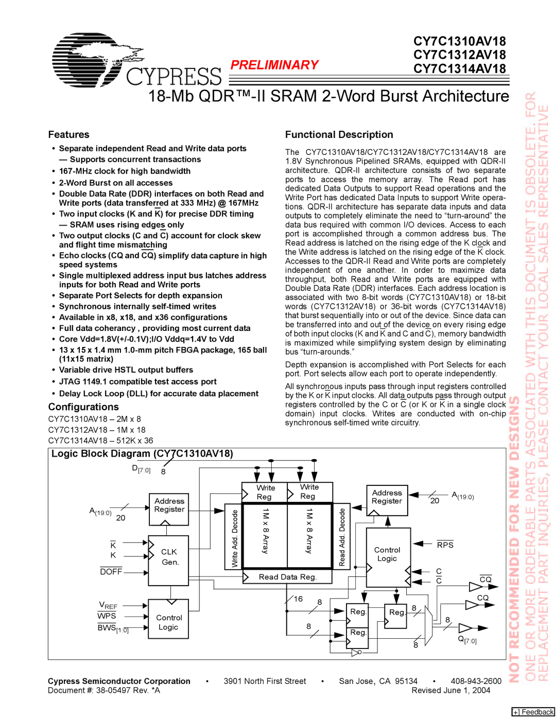
Functional Description
The CY7C1310AV18/CY7C1312AV18/CY7C1314AV18 are 1.8V Synchronous Pipelined SRAMs, equipped with
Depth expansion is accomplished with Port Selects for each port. Port selects allow each port to operate independently.
All synchronous inputs pass through input registers controlled by the K or K input clocks. All data outputs pass through output registers controlled by the C or C (or K or K in a single clock domain) input clocks. Writes are conducted with
Logic Block Diagram (CY7C1310AV18)
D[7:0] 8
A(19:0) 20
K
K
DOFF 

Address
Register ![]()
![]()
CLK
Gen.
| Write | Write |
|
|
|
|
|
|
|
|
|
|
|
|
|
| |
|
|
|
|
|
| Address |
|
|
|
| |||||||
| Reg | Reg |
|
|
|
|
|
|
|
|
| ||||||
|
|
|
|
|
| Register |
|
|
|
| |||||||
Decode | 1M x 8 | 1M x 8 | Decode |
|
|
|
|
|
|
|
|
|
|
|
|
| |
|
|
|
|
|
|
|
|
|
|
|
|
| |||||
|
|
|
|
|
|
|
|
|
|
|
|
| |||||
|
|
|
|
|
|
|
|
|
|
|
|
| |||||
Write Add. | Array | Array | Read Add. |
|
|
|
|
| Control |
|
|
| |||||
|
|
|
|
| Logic |
|
|
| |||||||||
| Read Data Reg. |
|
|
|
|
|
|
|
|
|
|
|
|
|
| ||
|
|
|
|
|
|
|
|
|
|
|
|
|
|
| |||
|
|
|
|
|
|
|
|
|
|
|
|
|
|
| |||
|
| 16 |
|
|
|
|
|
|
|
|
|
|
|
|
|
|
|
|
|
|
|
|
|
|
|
|
|
|
|
|
|
|
|
| |
|
|
|
|
|
|
|
|
|
|
|
|
|
|
|
|
| |
20A(19:0)
RPS
C
C |
|
| CQ | ||
| |||||
|
|
|
|
|
|
|
| CQ | |||
|
| ||||
VREF |
|
|
| |||
|
| |||||
WPS |
|
|
|
| Control | |
|
| |||||
BWS |
|
|
| Logic | ||
[1:0] |
| |||||
| 8 |
|
|
|
|
|
|
|
| 8 |
|
| Reg. |
|
|
| Reg. | ||||
|
|
|
|
|
|
| ||||
8 |
|
|
| |||||||
|
|
|
|
|
|
| ||||
|
|
|
|
|
|
|
|
|
| |
|
|
|
|
|
|
|
|
|
| |
|
|
|
|
|
|
|
|
|
| |
|
|
| Reg. |
|
|
|
| |||
|
|
|
|
|
|
|
| |||
|
|
|
|
|
|
|
|
| ||
|
|
|
|
|
|
|
| 8 | ||
|
|
|
|
|
|
| ||||
|
|
|
|
|
|
|
|
|
|
|
8
Q[7:0]
Cypress Semiconductor Corporation | • | 3901 North First Street | • | San Jose, CA 95134 | • | |
Document #: |
|
|
| Revised June 1, 2004 | ||
[+] Feedback