|
|
|
|
|
|
|
|
|
|
| CY7C1310AV18 | |
|
|
|
|
|
|
|
| PRELIMINARY | CY7C1312AV18 | |||
|
|
|
|
|
|
|
| CY7C1314AV18 | ||||
|
|
|
|
|
|
|
|
|
|
|
|
|
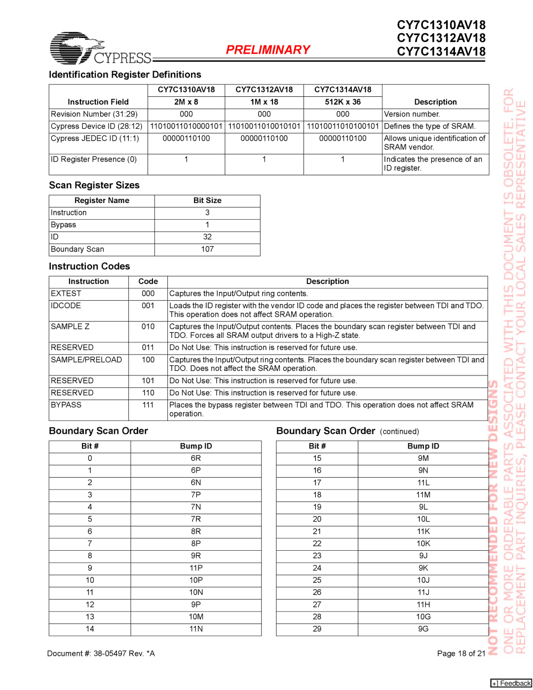
Identification Register Definitions |
|
|
|
|
| |||||||
|
|
|
|
|
|
|
|
|
|
|
| |
|
|
|
|
| CY7C1310AV18 | CY7C1312AV18 | CY7C1314AV18 |
|
| |||
Instruction Field |
|
|
|
|
|
|
|
|
| Description | ||
|
|
|
|
| 2M x 8 | 1M x 18 | 512K x 36 | |||||
Revision Number (31:29) |
|
|
|
| 000 | 000 | 000 | Version number. | ||||
|
|
|
|
|
|
|
|
| ||||
Cypress Device ID (28:12) | 11010011010000101 | 11010011010010101 | 11010011010100101 | Defines the type of SRAM. | ||||||||
|
|
|
|
|
|
|
|
|
| |||
Cypress JEDEC ID (11:1) |
|
|
| 00000110100 | 00000110100 | 00000110100 | Allows unique identification of | |||||
|
|
|
|
|
|
|
|
|
|
| SRAM vendor. | |
ID Register Presence (0) |
|
|
|
| 1 | 1 | 1 | Indicates the presence of an | ||||
|
|
|
|
|
|
|
|
|
|
| ID register. | |
Scan Register Sizes |
|
|
|
|
|
|
| |||||
|
|
|
|
|
|
|
|
|
|
|
|
|
Register Name |
|
|
|
|
| Bit Size |
|
|
|
|
| |
|
|
|
|
|
|
|
|
|
|
|
|
|
Instruction |
|
|
|
| 3 |
|
|
|
|
| ||
|
|
|
|
|
|
|
|
|
|
|
|
|
Bypass |
|
|
|
| 1 |
|
|
|
|
| ||
|
|
|
|
|
|
|
|
|
|
|
|
|
ID |
|
|
|
| 32 |
|
|
|
|
| ||
|
|
|
|
|
|
|
|
|
|
|
|
|
Boundary Scan |
|
|
|
| 107 |
|
|
|
|
| ||
|
|
|
|
|
|
|
|
|
|
|
|
|
Instruction Codes |
|
|
|
|
|
|
|
|
|
|
| |
|
|
|
|
|
|
|
|
|
| |||
Instruction |
| Code |
|
|
|
| Description |
|
| |||
|
|
|
|
|
|
|
| |||||
EXTEST |
| 000 |
|
| Captures the Input/Output ring contents. |
|
| |||||
|
|
|
|
|
| |||||||
IDCODE |
| 001 |
|
| Loads the ID register with the vendor ID code and places the register between TDI and TDO. | |||||||
|
|
|
|
|
|
| This operation does not affect SRAM operation. |
|
| |||
SAMPLE Z |
| 010 |
|
| Captures the Input/Output contents. Places the boundary scan register between TDI and | |||||||
|
|
|
|
|
|
| TDO. Forces all SRAM output drivers to a |
|
| |||
RESERVED |
| 011 |
|
| Do Not Use: This instruction is reserved for future use. |
|
| |||||
|
|
|
|
|
| |||||||
SAMPLE/PRELOAD |
| 100 |
|
| Captures the Input/Output ring contents. Places the boundary scan register between TDI and | |||||||
|
|
|
|
|
|
| TDO. Does not affect the SRAM operation. |
|
| |||
RESERVED |
| 101 |
|
| Do Not Use: This instruction is reserved for future use. |
|
| |||||
|
|
|
|
|
|
|
| |||||
RESERVED |
| 110 |
|
| Do Not Use: This instruction is reserved for future use. |
|
| |||||
|
|
|
|
|
| |||||||
BYPASS |
| 111 |
|
| Places the bypass register between TDI and TDO. This operation does not affect SRAM | |||||||
|
|
|
|
|
|
| operation. |
|
|
|
|
|
Boundary Scan Order
Bit # | Bump ID |
0 | 6R |
|
|
1 | 6P |
|
|
2 | 6N |
|
|
3 | 7P |
|
|
4 | 7N |
|
|
5 | 7R |
|
|
6 | 8R |
|
|
7 | 8P |
|
|
8 | 9R |
|
|
9 | 11P |
|
|
10 | 10P |
|
|
11 | 10N |
|
|
12 | 9P |
|
|
13 | 10M |
|
|
14 | 11N |
|
|
Document #:
Boundary Scan Order (continued)
Bit # | Bump ID |
15 | 9M |
|
|
16 | 9N |
|
|
17 | 11L |
|
|
18 | 11M |
|
|
19 | 9L |
|
|
20 | 10L |
|
|
21 | 11K |
|
|
22 | 10K |
|
|
23 | 9J |
|
|
24 | 9K |
|
|
25 | 10J |
|
|
26 | 11J |
|
|
27 | 11H |
|
|
28 | 10G |
|
|
29 | 9G |
|
|
Page 18 of 21
[+] Feedback