CY7C1310AV18
CY7C1312AV18
PRELIMINARYCY7C1314AV18
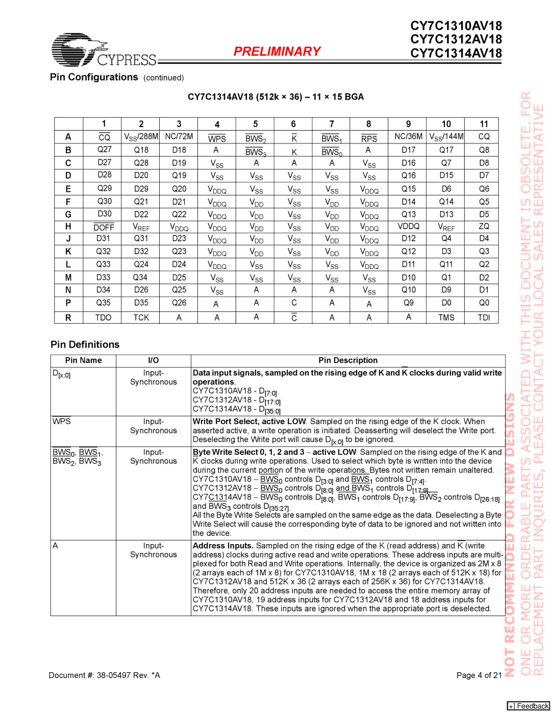
Pin Configurations (continued)
CY7C1314AV18 (512k × 36) – 11 × 15 BGA
| 1 |
|
| 2 | 3 | 4 |
| 5 |
| 6 |
|
| 7 |
| 8 |
| 9 | 10 | 11 | ||||||||
A |
|
|
|
|
| VSS/288M | NC/72M |
|
|
|
|
|
|
|
|
|
|
|
|
|
|
|
|
| NC/36M | VSS/144M | CQ |
|
| CQ |
|
|
| WPS |
|
| BWS | 2 |
|
| K |
|
|
| BWS | 1 |
| RPS |
| ||||||
B |
| Q27 | Q18 | D18 |
| A |
|
| 3 |
|
| K |
|
| 0 |
| A | D17 | Q17 | Q8 | |||||||
|
|
| BWS |
|
|
| BWS | ||||||||||||||||||||
C |
| D27 | Q28 | D19 |
| VSS |
| A |
|
| A |
| A |
| VSS | D16 | Q7 | D8 | |||||||||
D |
| D28 | D20 | Q19 |
| VSS |
| VSS | VSS |
| VSS |
| VSS | Q16 | D15 | D7 | |||||||||||
E |
| Q29 | D29 | Q20 | VDDQ |
| VSS | VSS |
| VSS | VDDQ | Q15 | D6 | Q6 | |||||||||||||
F |
| Q30 | Q21 | D21 | VDDQ |
| VDD | VSS |
| VDD | VDDQ | D14 | Q14 | Q5 | |||||||||||||
G |
| D30 | D22 | Q22 | VDDQ |
| VDD | VSS |
| VDD | VDDQ | Q13 | D13 | D5 | |||||||||||||
H |
|
|
| VREF | VDDQ | VDDQ |
| VDD | VSS |
| VDD | VDDQ | VDDQ | VREF | ZQ | ||||||||||||
| DOFF | ||||||||||||||||||||||||||
J |
| D31 | Q31 | D23 | VDDQ |
| VDD | VSS |
| VDD | VDDQ | D12 | Q4 | D4 | |||||||||||||
K |
| Q32 | D32 | Q23 | VDDQ |
| VDD | VSS |
| VDD | VDDQ | Q12 | D3 | Q3 | |||||||||||||
L |
| Q33 | Q24 | D24 | VDDQ |
| VSS | VSS |
| VSS | VDDQ | D11 | Q11 | Q2 | |||||||||||||
M |
| D33 | Q34 | D25 |
| VSS |
| VSS | VSS |
| VSS |
| VSS | D10 | Q1 | D2 | |||||||||||
N |
| D34 | D26 | Q25 |
| VSS |
| A |
|
| A |
| A |
| VSS | Q10 | D9 | D1 | |||||||||
P |
| Q35 | D35 | Q26 |
| A |
| A |
| C |
| A |
| A | Q9 | D0 | Q0 | ||||||||||
|
|
|
|
|
|
|
|
|
|
|
|
|
|
|
|
|
|
|
|
|
|
|
|
|
|
|
|
R |
| TDO | TCK | A |
| A |
| A |
|
|
|
| A |
| A | A | TMS | TDI | |||||||||
|
|
|
| C |
| ||||||||||||||||||||||
Pin Definitions
| Pin Name | I/O |
| Pin Description | ||||||||
| D[x:0] | Input- | Data input signals, sampled on the rising edge of K and | K | clocks during valid write | |||||||
|
|
|
|
| Synchronous | operations. |
|
|
|
|
|
|
|
|
|
|
|
| CY7C1310AV18 - D[7:0] |
|
|
|
|
|
|
|
|
|
|
|
| CY7C1312AV18 - D[17:0] |
|
|
|
|
|
|
|
|
|
|
|
| CY7C1314AV18 - D[35:0] |
|
|
|
|
|
|
| WPS |
|
|
| Input- | Write Port Select, active LOW. Sampled on the rising edge of the K clock. When | ||||||
|
|
|
|
| Synchronous | asserted active, a write operation is initiated. Deasserting will deselect the Write port. | ||||||
|
|
|
|
|
| Deselecting the Write port will cause D[x:0] to be ignored. | ||||||
| BWS | 0, | BWS | 1, | Input- | Byte Write Select 0, 1, 2 and 3 − active LOW. Sampled on the rising edge of the K and | ||||||
| BWS2, BWS3 | Synchronous | K clocks during write operations. Used to select which byte is written into the device | |||||||||
|
|
|
|
|
| during the current portion of the write operations. Bytes not written remain unaltered. | ||||||
|
|
|
|
|
| CY7C1310AV18 − BWS0 | controls D[3:0] and BWS1 | controls D[7:4]. | ||||
|
|
|
|
|
| CY7C1312AV18 − BWS0 | controls D[8:0] and BWS1 | controls D[17:9]. |
|
| ||
|
|
|
|
|
| CY7C1314AV18 − BWS0 | controls D[8:0], BWS1 controls D[17:9], BWS2 controls D[26:18] | |||||
|
|
|
|
|
| and BWS3 controls D[35:27]. |
|
|
|
|
| |
|
|
|
|
|
| All the Byte Write Selects are sampled on the same edge as the data. Deselecting a Byte | ||||||
|
|
|
|
|
| Write Select will cause the corresponding byte of data to be ignored and not written into | ||||||
|
|
|
|
|
| the device. |
|
|
|
|
|
|
| A | Input- | Address Inputs. Sampled on the rising edge of the K (read address) and | K | (write | |||||||
|
|
|
|
| Synchronous | address) clocks during active read and write operations. These address inputs are multi- | ||||||
|
|
|
|
|
| plexed for both Read and Write operations. Internally, the device is organized as 2M x 8 | ||||||
|
|
|
|
|
| (2 arrays each of 1M x 8) for CY7C1310AV18, 1M x 18 (2 arrays each of 512K x 18) for | ||||||
|
|
|
|
|
| CY7C1312AV18 and 512K x 36 (2 arrays each of 256K x 36) for CY7C1314AV18. | ||||||
|
|
|
|
|
| Therefore, only 20 address inputs are needed to access the entire memory array of | ||||||
|
|
|
|
|
| CY7C1310AV18, 19 address inputs for CY7C1312AV18 and 18 address inputs for | ||||||
|
|
|
|
|
| CY7C1314AV18. These inputs are ignored when the appropriate port is deselected. | ||||||
Document #: | Page 4 of 21 |
[+] Feedback