CY7C1317CV18, CY7C1917CV18

CY7C1319CV18, CY7C1321CV18

Switching Characteristics (continued)

Over the Operating Range [20, 21]

Cypress

Consortium


Description

300 MHz

278 MHz

250 MHz

200 MHz

167 MHz

Unit

Parameter

Parameter


Min

Max

Min

Max

Min

Max

Min

Max

Min

Max


Output Times


tCO

tCHQV

C/C

Clock Rise (or K/K in single

0.45

0.45

0.45

0.45

0.50

ns


clock mode) to Data Valid


tDOH

tCHQX


Data Output Hold after Output C/C


–0.45

–0.45

–0.45

–0.45

–0.50

ns


Clock Rise (Active to Active)


tCCQO

tCHCQV


Clock Rise to Echo Clock Valid

0.45

0.45

0.45

0.45

0.50

ns

C/C

tCQOH

tCHCQX


Echo Clock Hold after C/C

Clock

–0.45

–0.45

–0.45

–0.45

–0.50

ns


Rise


tCQD

tCQHQV

Echo Clock High to Data Valid

0.27

0.27

0.30

0.35

0.40

ns

tCQDOH

tCQHQX

Echo Clock High to Data Invalid

–0.27

–0.27

–0.30

–0.35

–0.40

ns

tCQH

tCQHCQL


HIGH [24]

1.24

1.35

1.55

1.95

2.45

ns

Output Clock (CQ/CQ)

tCQHCQH


tCQHCQH


CQ Clock Rise to


Clock Rise

1.24

1.35

1.55

1.95

2.45

ns


CQ


(rising edge to rising edge) [24]


tCHZ

tCHQZ


Clock (C/C)

Rise to High-Z

0.45

0.45

0.45

0.45

0.50

ns


(Active to High-Z) [25, 26]


tCLZ

tCHQX1


Rise to Low-Z [25, 26]


Clock (C/C)

–0.45

–0.45

–0.45

–0.45

–0.50

ns

DLL Timing


tKC Var

tKC Var

Clock Phase Jitter

0.20

0.20

0.20

0.20

0.20

ns

tKC lock

tKC lock

DLL Lock Time (K, C)

1024

1024

1024

1024

1024

Cycles

tKC Reset

tKC Reset

K Static to DLL Reset

30

30

30

30

30

ns

Notes

24.These parameters are extrapolated from the input timing parameters (tKHKH - 250 ps, where 250 ps is the internal jitter. An input jitter of 200 ps (tKC Var) is already included in the tKHKH). These parameters are only guaranteed by design and are not tested in production.

25.tCHZ, tCLZ are specified with a load capacitance of 5 pF as in (b) of AC Test Loads and Waveforms. Transition is measured ±100 mV from steady-state voltage.

26.At any voltage and temperature tCHZ is less than tCLZ and tCHZ less than tCO.

Document Number: 001-07161 Rev. *D

Page 25 of 31

[+] Feedback

Page 25
Image 25
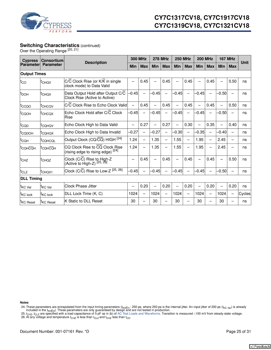
Cypress CY7C1319CV18, CY7C1321CV18, CY7C1317CV18, CY7C1917CV18 manual Parameter Min Max Output Times, DLL Timing

CY7C1321CV18, CY7C1917CV18, CY7C1319CV18, CY7C1317CV18 specifications

Cypress Semiconductor Corporation, a leading provider of advanced embedded memory solutions, offers a series of high-performance SRAM (Static Random Access Memory) devices ideal for a variety of applications. Among these devices are the CY7C1317CV18, CY7C1319CV18, CY7C1917CV18, and CY7C1321CV18. These components are designed to meet the growing demands for non-volatile memory in consumer electronics, automotive systems, telecommunications, and industrial applications.

The CY7C1317CV18 and CY7C1319CV18 are both 256K-bit static RAMs with distinct features. The CY7C1317CV18 offers a dual-port architecture, enabling concurrent access from multiple sources, which substantially enhances performance in data-intensive applications. On the other hand, the CY7C1319CV18 is designed for single-port access, making it ideal for simpler applications that do not require simultaneous data reads and writes.

Further extending Cypress's SRAM portfolio, the CY7C1917CV18 provides a 2M-bit memory configuration with fast access times, high-density storage, and low power consumption. It is particularly well-suited for applications needing quick data retrieval while maintaining efficiency. The architecture of the CY7C1917CV18 allows it to be integrated seamlessly into systems requiring reliable and robust data storage.

Completing the lineup is the CY7C1321CV18, which features an innovative 1M-bit SRAM design. This SRAM is known for its low latency and high speed, making it an excellent choice for high-performance computing applications. It supports a wide operating voltage range and provides a reliable solution for volatile memory needs, especially in fast caching scenarios.

These SRAM devices utilize advanced CMOS technology to achieve high speed and low power characteristics, making them competitive choices in the market. Their robust performance ensures that they satisfy the stringent requirements of various applications, including high-speed networking, graphics processing, and instrumentation.

In terms of reliability, all four devices are built to endure challenging operating conditions and provide excellent data retention. They are offered in compact packages that facilitate easy integration into PCBs, optimizing space and enhancing design flexibility. The combination of performance, low power consumption, and scalability makes Cypress's SRAM products particularly advantageous for next-generation applications across multiple industries.