|
|
|
|
|
|
|
|
|
|
|
|
|
|
|
|
|
|
|
|
|
|
|
|
|
|
|
| CY7C1338G | |
|
|
|
|
|
|
|
|
|
|
|
|
|
|
|
|
|
|
|
|
|
|
|
|
|
|
|
| ||
|
|
|
|
|
|
|
|
|
|
|
|
|
|
|
|
|
|
|
|
|
|
|
|
|
|
|
|
|
|
|
|
|
|
|
|
|
|
|
|
|
|
|
|
|
|
|
|
|
|
|
|
|
|
|
|
|
|
|
|
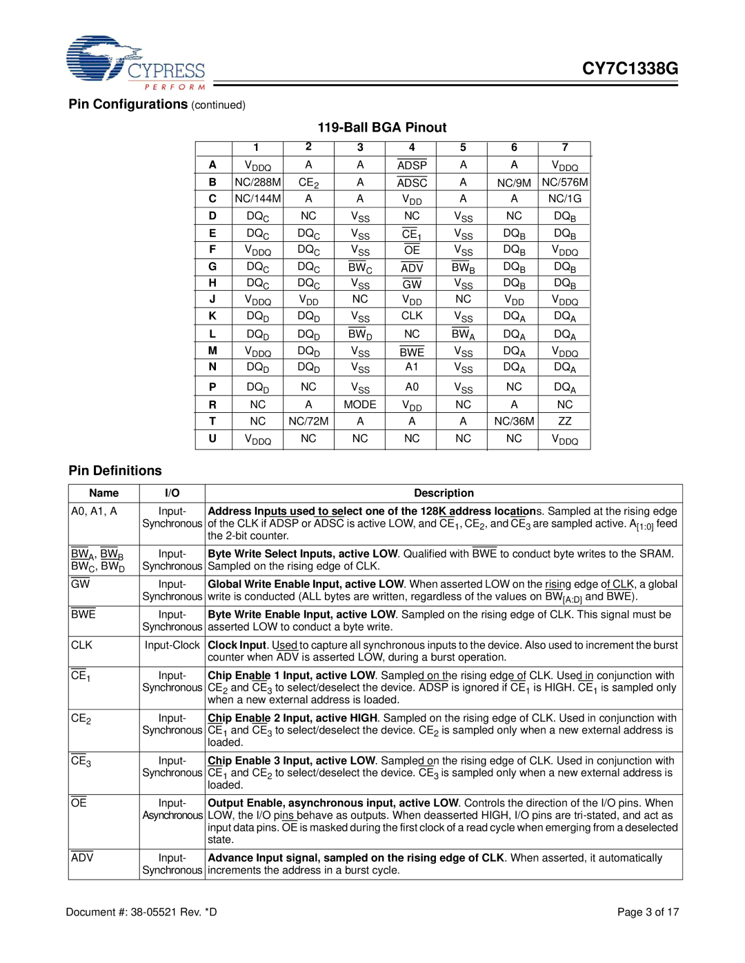
Pin Configurations (continued) |
|
|
|
|
|
|
|
|
|
|
|
|
|
|
|
|
|
|
|
|
|
|
|
| |||||
|
|
|
|
|
|
|
|
|
|
|
|
| |||||||||||||||||
|
|
|
|
|
|
|
|
|
|
|
|
|
|
|
|
|
|
|
|
|
|
|
|
|
|
|
|
|
|
|
|
|
|
| 1 | 2 | 3 |
| 4 |
|
|
|
|
|
|
|
| 5 |
|
| 6 | 7 |
| ||||||
|
|
| A | VDDQ | A |
| A |
|
|
|
|
|
|
|
|
|
|
|
|
|
| A | A | VDDQ |
| ||||
|
|
|
| ADSP |
|
| |||||||||||||||||||||||
|
|
| B | NC/288M | CE2 |
| A |
|
|
|
|
|
|
|
|
|
|
|
|
| A | NC/9M | NC/576M |
| |||||
|
|
|
| ADSC |
|
| |||||||||||||||||||||||
|
|
| C | NC/144M | A |
| A |
|
|
| VDD |
| A | A | NC/1G |
| |||||||||||||
|
|
| D | DQC | NC |
| VSS |
|
|
|
|
| NC |
| VSS | NC | DQB |
| |||||||||||
|
|
| E | DQC | DQC |
| VSS |
|
|
|
|
|
| 1 |
|
|
| VSS | DQB | DQB |
| ||||||||
|
|
|
|
|
| CE |
|
| |||||||||||||||||||||
|
|
| F | VDDQ | DQC |
| VSS |
|
|
|
|
|
|
|
|
|
|
| VSS | DQB | VDDQ |
| |||||||
|
|
|
|
|
|
|
| OE |
|
| |||||||||||||||||||
|
|
| G | DQC | DQC |
|
| C |
|
|
|
|
|
|
|
|
|
|
| B | DQB | DQB |
| ||||||
|
|
| BW |
|
|
| ADV |
|
|
| BW |
| |||||||||||||||||
|
|
| H | DQC | DQC |
| VSS |
|
|
|
|
|
|
|
| VSS | DQB | DQB |
| ||||||||||
|
|
|
|
|
|
| GW |
|
| ||||||||||||||||||||
|
|
| J | VDDQ | VDD |
| NC |
|
|
| VDD |
| NC | VDD | VDDQ |
| |||||||||||||
|
|
| K | DQD | DQD |
| VSS |
|
|
| CLK |
| VSS | DQA | DQA |
| |||||||||||||
|
|
| L | DQD | DQD |
|
| D |
|
|
|
|
| NC |
|
| A | DQA | DQA |
| |||||||||
|
|
|
| BW |
|
|
|
|
|
| BW |
| |||||||||||||||||
|
|
| M | VDDQ | DQD |
| VSS |
|
|
|
|
| VSS | DQA | VDDQ |
| |||||||||||||
|
|
|
|
|
| BWE |
|
| |||||||||||||||||||||
|
|
| N | DQD | DQD |
| VSS |
|
|
|
|
| A1 |
| VSS | DQA | DQA |
| |||||||||||
|
|
| P | DQD | NC |
| VSS |
|
|
|
|
| A0 |
| VSS | NC | DQA |
| |||||||||||
|
|
| R | NC | A | MODE |
|
|
| VDD |
| NC | A | NC |
| ||||||||||||||
|
|
| T | NC | NC/72M |
| A |
|
|
|
|
| A |
| A | NC/36M | ZZ |
| |||||||||||
|
|
| U | VDDQ | NC |
| NC |
|
|
|
|
| NC |
| NC | NC | VDDQ |
| |||||||||||
Pin Definitions
|
|
|
| Name | I/O |
|
| Description | |||||||
|
|
|
| ||||||||||||
| A0, A1, A | Input- | Address Inputs used to select one of the 128K address locations. Sampled at the rising edge | ||||||||||||
|
|
|
|
|
|
|
|
|
| Synchronous | of the CLK if ADSP or | ADSC | is active LOW, and CE1, CE2, and CE3 are sampled active. A[1:0] feed | ||
|
|
|
|
|
|
|
|
|
|
| the | ||||
|
|
|
| A, |
| B | Input- | Byte Write Select Inputs, active LOW. Qualified with |
| to conduct byte writes to the SRAM. | |||||
| BW | BW | BWE | ||||||||||||
| BWC, BWD | Synchronous | Sampled on the rising edge of CLK. | ||||||||||||
|
|
|
|
|
|
|
| Input- | Global Write Enable Input, active LOW. When asserted LOW on the rising edge of CLK, a global | ||||||
| GW | ||||||||||||||
|
|
|
|
|
|
|
|
|
| Synchronous | write is conducted (ALL bytes are written, regardless of the values on BW[A:D] and BWE). | ||||
|
|
|
|
|
|
|
| Input- | Byte Write Enable Input, active LOW. Sampled on the rising edge of CLK. This signal must be | ||||||
| BWE | ||||||||||||||
|
|
|
|
|
|
|
|
|
| Synchronous | asserted LOW to conduct a byte write. | ||||
| CLK | Clock Input. Used to capture all synchronous inputs to the device. Also used to increment the burst | |||||||||||||
|
|
|
|
|
|
|
|
|
|
| counter when ADV is asserted LOW, during a burst operation. | ||||
|
| 1 |
| Input- | Chip Enable 1 Input, active LOW. Sampled on the rising edge of CLK. Used in conjunction with | ||||||||||
| CE | ||||||||||||||
|
|
|
|
|
|
|
|
|
| Synchronous | CE2 and CE3 to select/deselect the device. ADSP is ignored if CE1 is HIGH. CE1 is sampled only | ||||
|
|
|
|
|
|
|
|
|
|
| when a new external address is loaded. | ||||
| CE2 | Input- | Chip Enable 2 Input, active HIGH. Sampled on the rising edge of CLK. Used in conjunction with | ||||||||||||
|
|
|
|
|
|
|
|
|
| Synchronous | CE1 and CE3 to select/deselect the device. CE2 is sampled only when a new external address is | ||||
|
|
|
|
|
|
|
|
|
|
| loaded. | ||||
|
| 3 |
| Input- | Chip Enable 3 Input, active LOW. Sampled on the rising edge of CLK. Used in conjunction with | ||||||||||
| CE | ||||||||||||||
|
|
|
|
|
|
|
|
|
| Synchronous | CE1 and CE2 to select/deselect the device. CE3 is sampled only when a new external address is | ||||
|
|
|
|
|
|
|
|
|
|
| loaded. | ||||
|
|
|
|
| Input- | Output Enable, asynchronous input, active LOW. Controls the direction of the I/O pins. When | |||||||||
| OE | ||||||||||||||
|
|
|
|
|
|
|
|
|
| Asynchronous | LOW, the I/O pins behave as outputs. When deasserted HIGH, I/O pins are | ||||
|
|
|
|
|
|
|
|
|
|
| input data pins. OE is masked during the first clock of a read cycle when emerging from a deselected | ||||
|
|
|
|
|
|
|
|
|
|
| state. | ||||
|
|
|
|
|
|
| Input- | Advance Input signal, sampled on the rising edge of CLK. When asserted, it automatically | |||||||
| ADV | ||||||||||||||
|
|
|
|
|
|
|
|
|
| Synchronous | increments the address in a burst cycle. | ||||
Document #: | Page 3 of 17 |